ZHCS901E May 2012 – September 2021 TPS55340
PRODUCTION DATA
- 1 特性
- 2 应用
- 3 说明
- 4 Revision History
- 5 Pin Configuration and Functions
- 6 Specifications
- 7 Detailed Description
-
8 Application and Implementation
- 8.1 Application Information
- 8.2
Typical Applications
- 8.2.1
Boost Converter
- 8.2.1.1 Design Requirements
- 8.2.1.2
Detailed Design Procedure
- 8.2.1.2.1 Custom Design with WEBENCH Tools
- 8.2.1.2.2 Selecting the Switching Frequency (R4)
- 8.2.1.2.3 Determining the Duty Cycle
- 8.2.1.2.4 Selecting the Inductor (L1)
- 8.2.1.2.5 Computing the Maximum Output Current
- 8.2.1.2.6 Selecting the Output Capacitors (C8, C9, C10)
- 8.2.1.2.7 Selecting the Input Capacitors (C2, C7)
- 8.2.1.2.8 Setting Output Voltage (R1, R2)
- 8.2.1.2.9 Setting the Soft-start Time (C7)
- 8.2.1.2.10 Selecting the Schottky Diode (D1)
- 8.2.1.2.11 Compensating the Control Loop (R3, C4, C5)
- 8.2.1.3 Application Curves
- 8.2.2
SEPIC Converter
- 8.2.2.1 Design Requirements
- 8.2.2.2
Detailed Design Procedure
- 8.2.2.2.1 Selecting the Switching Frequency (R4)
- 8.2.2.2.2 Duty Cycle
- 8.2.2.2.3 Selecting the Inductor (L1)
- 8.2.2.2.4 Calculating the Maximum Output Current
- 8.2.2.2.5 Selecting the Output Capacitors (C8, C9, C10)
- 8.2.2.2.6 Selecting the Series Capacitor (C6)
- 8.2.2.2.7 Selecting the Input Capacitor (C2, C7)
- 8.2.2.2.8 Selecting the Schottky Diode (D1)
- 8.2.2.2.9 Setting the Output Voltage (R1, R2)
- 8.2.2.2.10 Setting the Soft-start Time (C3)
- 8.2.2.2.11 MOSFET Rating Considerations
- 8.2.2.2.12 Compensating the Control Loop (R3, C4)
- 8.2.2.3 Application Curves
- 8.2.1
Boost Converter
- 9 Power Supply Recommendations
- 10Layout
- 11Device and Documentation Support
- 12Mechanical, Packaging, and Orderable Information
8.2.1.2.11 Compensating the Control Loop (R3, C4, C5)
The TPS55340 requires external compensation which allows the loop response to be optimized for each application. The COMP pin is the output of the internal error amplifier. An external resistor R3 and ceramic capacitor C4 are connected to the COMP pin to provide a pole and a zero, shown in Figure 8-1. This pole and zero, along with the inherent pole and zero of a boost converter, determine the closed-loop frequency response. This is important for converter stability and transient response. Loop compensation should be designed for the minimum operating voltage.
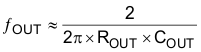
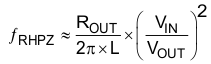
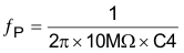
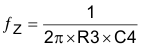
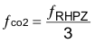
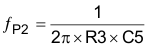
The following equations summarize the loop equations for the TPS55340 configured as a CCM boost converter. They include the power stage output pole (ƒOUT) and the right-half-plane zero (ƒRHPZ) of a boost converter calculated with Equation 27 and Equation 28, respectively. When calculating ƒOUT, it is important to include the derating of ceramic output capacitors. In the example with an estimated 10.2-µF capacitance, these frequencies are calculated to be 980 kHz and 22.1 kHz, respectively. The dc gain (A) of the power stage is calculated with Equation 29 and is 39.9 dB in this design. The compensation pole (ƒP) and zero (ƒZ) generated by R3, C4, and internal transconductance amplifier are calculated with Equation 30 and Equation 31, respectively.
Most CCM boost converters will have a stable control loop if fZ is set slightly above ƒP through proper sizing of R3 and C4. A good starting point is C4 = 0.1 µF and R3 = 2 kΩ. Increasing R3 or reducing C4 increases the closed-loop bandwidth, and therefore improves the transient response. Adjusting R3 and C4 in the opposite direction increases the phase and gain margin of the loop, which improves loop stability. It is generally recommended to limit the bandwidth of the loop to the lower of either 1/5 of the switching frequency ƒSW or 1/3 the RHPZ frequency, ƒRHPZ shown in Equation 28. The spreadsheet tool located in the TPS55340 product folder at www.ti.com can also be used to aid in compensation design.
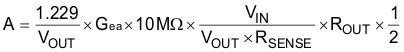

where
- COUT is the equivalent output capacitor (COUT= C8 + C9 + C10)
- ROUT is the equivalent load resistance (VOUT/IOUT)
- Gea is the error amplifier transconductance located in Section 6.5
- RSENSE (15 mΩ, typical) is the sense resistor in the current control loop
- ƒco1 and ƒco2 are possible bandwidths.
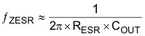
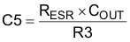
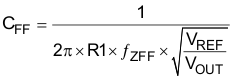
An additional capacitor from the COMP pin to GND (C5) can be used to place a high-frequency pole in the control loop. This is not always necessary with ceramic output capacitors. If a nonceramic output capacitor is used, there is an additional zero (fZESR) in the control loop which can be calculated with Equation 35. The value of C5 and the pole created by C5 can be calculated with Equation 36 and Equation 34, respectively. Finally, if more phase margin is needed, an additional zero (fZFF) can be added by placing a capacitor (CFF) in parallel with the top feedback resistor R1. It is recommended to place the zero at the target cross-over frequency or higher. The feed-forward capacitor also adds a pole at a higher frequency. The recommended value of CFF can be calculated with Equation 37.
where
- RESR is the ESR of the output capacitor
If a network measurement tool is available, the most accurate compensation design can be achieved following this procedure. The power stage frequency response is first measured using a network analyzer at the minimum 5-V input and maximum 800-mA load. This measurement is shown in Figure 8-2. In this design only one pole and one zero are used, so the maximum phase increase from the compensation will be 180 degrees. For a
60-degree phase margin, the power stage phase must be –120 degrees at its lowest point. Based on the target 6-kHz bandwidth, the measured power stage gain, KPS(fBW), is 24.84 dB and the phase is –110.3 degrees.
 Figure 8-2 Power Stage Gain and Phase of the Boost Converter
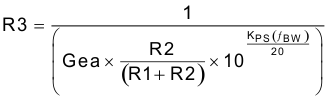
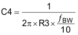
R3 is then chosen to set the compensation gain to be the reciprocal of the power stage gain at the target bandwidth using Equation 38. C4 is then chosen to place a zero at 1/10 the target bandwidth with Equation 39. In this case, R3 is calculated to be 2.56 kΩ and the nearest standard value of 2.55 kΩ is used. C4 is calculated at 0.104 µF and the nearest standard value of 0.100 µF is used. Although not necessary because this design uses all ceramic capacitors, a 100-pF capacitor is selected for C5 to add a high-frequency pole at a frequency 100 times the target bandwidth.