-
适用于 EV 和 HEV 的 bq76PL536A-Q1 3 至 6 节锂离子电池监控器和二级保护 IC单元
- 1 特性
- 2 应用
- 3 说明
- 4 修订历史记录
- 5 Pin Configuration and Functions
- 6 Specifications
-
7 Detailed Description
- 7.1 Overview
- 7.2 Functional Block Diagram
- 7.3
Feature Description
- 7.3.1
Analog-to-Digital Conversion (ADC)
- 7.3.1.1 General Features
- 7.3.1.2 3-to-6 Series Cell Configuration
- 7.3.1.3 Cell Voltage Measurements
- 7.3.1.4 GPAI or VBAT Measurements
- 7.3.1.5 Temperature Measurement
- 7.3.1.6 ADC Band-Gap Voltage Reference
- 7.3.1.7 Conversion Control
- 7.3.1.8 Secondary Protection
- 7.3.1.9 Cell Overvoltage Fault Detection (COV)
- 7.3.1.10 Cell Undervoltage Fault Detection (CUV)
- 7.3.1.11 Overtemperature Detection
- 7.3.1.12 Fault and Alert Behavior
- 7.3.1.13 Secondary Protector Built-In Self-Test Features
- 7.3.2 Cell Balancing
- 7.3.3 Other Features and Functions
- 7.3.4 Communications
- 7.3.1
Analog-to-Digital Conversion (ADC)
- 7.4 Device Functional Modes
- 7.5 Programming
- 7.6
Register Maps
- 7.6.1 I/O Register Details
- 7.6.2 Register Types
- 7.6.3
Register Details
- 7.6.3.1 DEVICE_STATUS Register (0x00)
- 7.6.3.2 GPAI (0x01, 0x02) Register
- 7.6.3.3 VCELLn Register (0x03…0x0e)
- 7.6.3.4 TEMPERATURE1 Register (0x0f, 0x10)
- 7.6.3.5 TEMPERATURE2 Register (0x11, 0x12)
- 7.6.3.6 ALERT_STATUS Register (0x20)
- 7.6.3.7 FAULT_STATUS Register (0x21)
- 7.6.3.8 COV_FAULT Register (0x22)
- 7.6.3.9 CUV_FAULT Register (0x23)
- 7.6.3.10 PARITY_H Register (0x24) [PRESULT_A (R/O)]
- 7.6.3.11 PARITY_H Register (0x25) [PRESULT_B (R/O)]
- 7.6.3.12 ADC_CONTROL Register (0x30)
- 7.6.3.13 IO_CONTROL Register (0x31)
- 7.6.3.14 CB_CTRL Register (0x32)
- 7.6.3.15 CB_TIME Register (0x33)
- 7.6.3.16 ADC_CONVERT Register (0x34)
- 7.6.3.17 SHDW_CTRL Register (0x3a)
- 7.6.3.18 ADDRESS_CONTROL Register (0x3b)
- 7.6.3.19 RESET Register (0x3c)
- 7.6.3.20 TEST_SELECT Register (0x3d)
- 7.6.3.21 E_EN Register (0x3f)
- 7.6.3.22 FUNCTION_CONFIG Register (0x40)
- 7.6.3.23 IO_CONFIG Register (0x41)
- 7.6.3.24 CONFIG_COV Register (0x42)
- 7.6.3.25 CONFIG_COVT Register (0x43)
- 7.6.3.26 CONFIG_UV Register (0x44)
- 7.6.3.27 CONFIG_CUVT Register (0x45)
- 7.6.3.28 CONFIG_OT Register (0x46)
- 7.6.3.29 CONFIG_OTT Register (0x47)
- 7.6.3.30 USERx Register (0x48-0x4b) (USER1-4)
- 8 Application and Implementation
- 9 Power Supply Recommendations
- 10Layout
- 11器件和文档支持
- 12机械、封装和可订购信息
- 重要声明
适用于 EV 和 HEV 的 bq76PL536A-Q1 3 至 6 节锂离子电池监控器和二级保护 IC单元
1 特性
- 符合汽车应用 应用认证
- 具有符合 AEC-Q100 标准的下列结果:
- 器件温度 2 级:-40℃ 至 +105℃ 的环境运行温度范围
- 器件人体模型 (HBM) 分类等级 2
- 器件充电器件模型 (CDM) 分类等级 C4B
- 3 节至 6 节电池支持,所有化合物
- 热插拔
- 用于数据通信的高速串行外设接口 (SPI)
- 支持垂直堆叠的接口
- 器件之间无需隔离组件
- 高精度模数转换器 (ADC):
- ±1mV 典型精度
- 14 位分辨率,6µs 转换时间
- 九个 ADC 输入
- 支持同步测量的专用引脚
- 配置数据存储在具有差错校验/纠正 (ECC) 功能的一次性可编程 (OTP) 寄存器中
- 内置比较器(二级保护器)支持:
- 过压和欠压保护
- 过热保护
- 可编程的阈值和延迟时间
- 专用故障信号
- 支持安全超时功能的电芯均衡控制输出
- 通过外部组件设置均衡电流
- 电源电压范围:7.2V 至 27V 连续电压以及 36V 峰值
- 低功耗:
- 休眠电流典型值为 12µA,空闲电流典型值为 45µA
- 集成 5V、3mA 高精度 LDO
2 应用
- 电动车与混合动力电动车
- 不间断电源系统 (UPS)
- 电动自行车和电动踏板车
- 大型电池系统
3 说明
bq76PL536A-Q1 器件是用于三至六节串联锂离子电池的可堆叠电池监控器和保护器。bq76PL536A-Q1 集成了模拟前端 (AFE) 以及精密模数转换器 (ADC),用于精确测量电池电压。使用一个单独的 ADC 来测量温度。
除测量温度外,该器件还对各通道提供过压和欠压监控保护。通过非易失性存储器来存储用户可编程的保护阈值和延迟时间。一旦超出其中某个阈值,就会输出故障信号。
可通过堆叠式 bq76PL536A-Q1 器件来实现对由 192 节电池组成的电池组的支持。所有器件通过高速 SPI 接口进行连接。
器件信息(1)
| 器件型号 | 封装 | 封装尺寸(标称值) |
|---|---|---|
| bq76PL536A-Q1 | HTQFP (64) | 10.00mm x 10.00mm |
- 如需了解所有可用封装,请见数据表末尾的可订购产品附录。
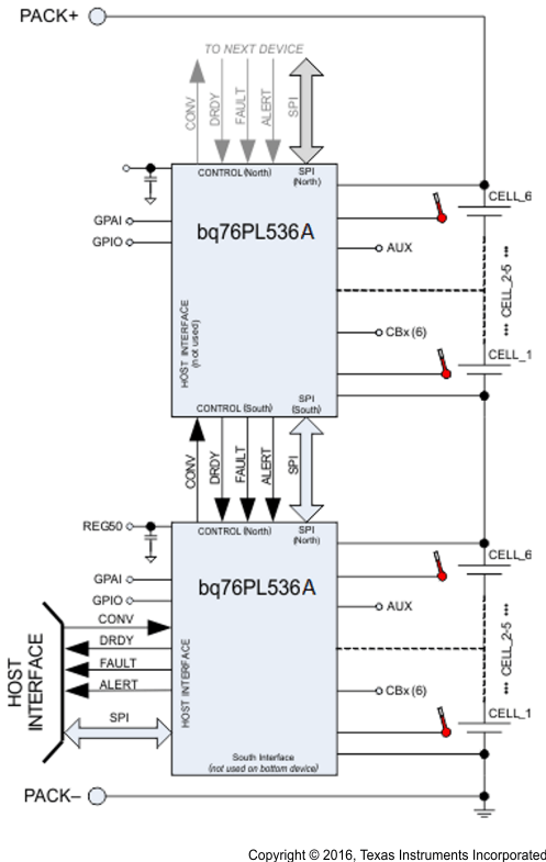
简化的系统连接
4 修订历史记录
Changes from * Revision (May 2011) to A Revision
- Added ESD 额定值表,特性 描述部分,器件功能模式,应用和实施部分,电源相关建议部分,布局部分,器件和文档支持部分以及机械、封装和可订购信息部分Go
- Changed 将电源电压范围从“6V 至 30V”更改为“7.2V 至 27V”(特性部分) Go
- Changed 描述 以使其更为简洁Go
- Changed graphic pin 54 alignment and part number Go
- Changed AUX description Go
- Listed values and removed VCn to VCn-1 row and updated Input Voltage Range and Output Voltage Range informationGo
- Changed "VBAT = 20 V" to "VBAT = 22 V" throughout data sheetGo
- Changed value to 27 VGo
- Combined Electrical Characteristics tables into one table Go
- Changed lower range to 7.2 Go
- Changed format of bottom two rows and added notes Go
- Deleted MAX value for VIHGo
- Deleted MIN value for VILGo
- Changed 120 to 125Go
- Changed test conditionGo
- Deleted note Go
- Added error range Go
- Changed table values and format Go
- Changed min valueGo
- Changed test conditions, Min and Nom values, and added note 4 Go
- Changed the section to be switching characteristics Go
- Changed units in equations to match unit in corresponding row Go
- Moved figure after timing requirements Go
- Changed name from VC0 to VSS Go
- Added TNOM table note Go
- Changed note wording for LDODxGo
- Changed warning to cautionGo
- Changed text to a warningGo
- Changed text to a caution and added SLEEP State in textGo
- Changed TS1(2) to TS1:TS2 throughout documentGo
- Changed SHADOW_LOAD to REFRESH Go
- Changed paragraph text and added cross-reference to section Go
- Changed definition of 1 value Go
- Changed text to Caution format.Go
- Changed anti-aliasing VCn input to VC6-VC1Go
- Changed "SN76PL536-Q1" to "bq76PL536A-Q1" in Power Supply DecouplingGo
- Changed note wording for LDODxGo
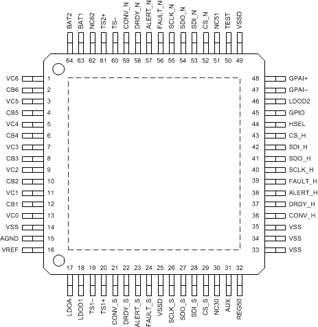
5 Pin Configuration and Functions
Pin Functions
| PIN | TYPE(1) | DESCRIPTION | |
|---|---|---|---|
| NAME | NO. | ||
| AGND | 15 | AI | Internal analog VREF (–) |
| ALERT_H | 38 | O | Host-to-device interface – ALERT condition detected in this or higher (North) device |
| ALERT_N | 57 | I | Current-mode input indicating a system status change from the next-higher bq76PL536A-Q1 |
| ALERT_S | 23 | OD | Current-mode output indicating a system status change to the next lower bq76PL536A-Q1 |
| AUX | 31 | O | Switched current-limited output from REG50 |
| BAT1 | 63 | P | Power-supply voltage, connect to most-positive cell +, tie to BAT2 on PCB |
| BAT2 | 64 | P | Power-supply voltage, connect to most-positive cell +, tie to BAT1 on PCB |
| CB1 | 12 | O | Cell-balance control output 1 |
| CB2 | 10 | O | Cell-balance control output 2 |
| CB3 | 8 | O | Cell-balance control output 3 |
| CB4 | 6 | O | Cell-balance control output 4 |
| CB5 | 4 | O | Cell-balance control output 5 |
| CB6 | 2 | O | Cell-balance control output 6 |
| CONV_H | 36 | I | Host-to-device interface – initiates a synchronous conversion. Pin has 250-nA internal sink to VSS. |
| CONV_N | 59 | OD | Current-mode output to the next-higher bq76PL536A-Q1 to initiate a conversion |
| CONV_S | 21 | I | Input from the adjacent lower bq76PL536A-Q1 to initiate a conversion |
| CS_H | 43 | I | Host-to-device interface – active-low chip select from host. Internal 100-kΩ pull-up resistor |
| CS_N | 52 | OD | Current-mode output used to select the next-higher bq76PL536A-Q1 for SPI communication |
| CS_S | 29 | I | Current-mode input SPI chip-select (slave-select) from the next-lower bq76PL536A-Q1 |
| DRDY_H | 37 | O | Host-to-device interface – conversion complete, data-ready indication |
| DRDY_N | 58 | I | Current-mode input indicating conversion data is ready from next-higher bq76PL536A-Q1 |
| DRDY_S | 22 | OD | Current-mode output indicating conversion data is ready to the next lower bq76PL536A-Q1 |
| FAULT_H | 39 | O | Host-to-device interface – FAULT condition detected in this or higher (North) device |
| FAULT_N | 56 | I | Current-mode input indicating a system status change from the next-higher bq76PL536A-Q1 |
| FAULT_S | 24 | OD | Current-mode output |
| GPAI+ | 48 | AI | General-purpose (differential) analog input, connect to VSS if unused. |
| GPAI– | 47 | AI | General-purpose (differential) analog input, connect to VSS if unused. |
| GPIO | 45 | IOD | Digital open-drain I/O. A 10-kΩ to 2-MΩ pull-up is recommended. |
| HSEL | 44 | I | Host interface enable, 0 = enable, 1 = disable |
| LDOA | 17 | P | Internal analog 5-V LDO bypass connection, requires 2.2-µF ceramic capacitor for stability |
| LDOD1 | 18 | P | Internal digital 5-V LDO bypass connection 1, requires 2.2-µF ceramic capacitor for stability. This pin is tied internally to LDOD2. This pin should be tied to LDOD2 externally. |
| LDOD2 | 46 | P | Internal digital 5-V LDO bypass connection 2, requires 2.2-µF ceramic capacitor for stability. This pin is tied internally to LDOD1. This pin should be tied to LDOD1 externally. |
| NC30 | 30 | — | No connection |
| NC51 | 51 | — | No connection |
| NC62 | 62 | — | No connection |
| REG50 | 32 | P | 5-V user LDO output, requires 2.2-µF ceramic capacitor for stability |
| SCLK_H | 40 | I | Host-to-device interface – SPI clock from host |
| SCLK_N | 55 | OD | Current-mode output SPI clock to the next-higher bq76PL536A-Q1 |
| SCLK_S | 26 | I | Current-mode input SPI clock from the next-lower bq76PL536A-Q1 |
| SDI_H | 42 | I | Host-to-device interface – data from host to device (host MOSI signal) |
| SDI_N | 53 | OD | Current-mode output for SPI data to the next-higher bq76PL536A-Q1 |
| SDI_S | 28 | I | Current-mode input for SPI data from the next-lower bq76PL536A-Q1 |
| SDO_H | 41 | O | Host-to-device interface – data from device to host (host MISO signal), 3-state pin, 250-nA internal pull-up |
| SDO_N | 54 | I | Current-mode input for SPI data from the next-lower bq76PL536A-Q1 |
| SDO_S | 27 | OD | Current-mode output for SPI data to the next-lower bq76PL536A-Q1 |
| TEST | 50 | I | Factory test pin. Connect to VSS in user circuitry. This pin includes an approximately 100-kΩ internal pull-down |
| TS1+ | 20 | AI | Differential temperature sensor input |
| TS1– | 19 | AI | Differential temperature sensor input |
| TS2+ | 61 | AI | Differential temperature sensor input |
| TS2– | 60 | AI | Differential temperature sensor input |
| VC0 | 13 | AI | Sense-voltage input terminal for negative terminal of first cell (VSS) |
| VC1 | 11 | AI | Sense voltage input terminal for positive terminal of the first cell |
| VC2 | 9 | AI | Sense voltage input terminal for the positive terminal of the second cell |
| VC3 | 7 | AI | Sense voltage input terminal for the positive terminal of the third cell |
| VC4 | 5 | AI | Sense voltage input terminal for the positive terminal of the fourth cell |
| VC5 | 3 | AI | Sense voltage input terminal for the positive terminal of the fifth cell |
| VC6 | 1 | AI | Sense voltage input terminal for the positive terminal of the sixth cell |
| VREF | 16 | P | Internal analog voltage reference (+), requires 10-µF, low-ESR ceramic capacitor to AGND for stability |
| VSS | 14, 33, 34, 35 | P | VSS |
| VSSD | 25, 49 | P | VSS |
| Thermal pad | — | — | Thermal pad on bottom of PowerPAD™ package; this must be soldered to similar-size copper area on PCB and connected to VSS, to meet stated specifications herein. Provides heat-sinking to part. |
- Key: I = digital input, AI = analog input, O = digital output, OD = open-drain output, T = 3-state output, P = power.
6 Specifications
6.1 Absolute Maximum Ratings
over operating free-air temperature range (unless otherwise noted) (1)| MIN | MAX | UNIT | |||
|---|---|---|---|---|---|
| VMAX | Supply voltage | BAT1, BAT2(2) | –0.3 | 36 | V |
| VIN | Input voltage | VC1, VC2, VC3, VC4, VC5, VC6 | –0.3 | 36 | V |
| VC0 | –0.3 | 2 | |||
| TS1+, TS1–, TS2+, TS2– | –0.3 | 6 | |||
| GPAI | –0.3 | 6 | |||
| GPIO | –0.3 | VREG50 + 0.3 | |||
| DRDY_N, SDO_N, FAULT_N, ALERT_N | VBAT – 1 | VBAT + 2 | |||
| CONV_H, SDI_H, SCLK_H, CS_H | –0.3 | 6 | |||
| CONV_S, SDI_S, SCLK_S, CS_S | –2 | 1 | |||
| VO | Output voltage | CONV_N, SDI_N, SCLK_N, CS_N | –0.3 | 36 | V |
| SDO_H, FAULT_H, ALERT_H, DRDY_H | –0.3 | 6 | |||
| DRDY_S, SDO_S, FAULT_S, ALERT_S | –0.3 | 5 | |||
| GPIO | –0.3 | VREG50 + 0.3 | |||
| CB1…CB6 (CBREF = 0x00) | –0.3 | 36 | |||
| REG50, AUX | –0.3 | 6 | |||
| TJ | Junction temperature | 150 | °C | ||
| Tstg | Storage temperature | –65 | 150 | °C | |
6.2 ESD Ratings
| VALUE | UNIT | ||||
|---|---|---|---|---|---|
| V(ESD) | Electrostatic discharge | Human-body model (HBM), per AEC Q100-002(1) | ±2000 | V | |
| Charged-device model (CDM), per AEC Q100-011 | All pins | ±500 | |||
| Corner pins (1,16, 33, and 48) | ±750 | ||||
6.3 Recommended Operating Conditions
Typical values stated where TA = 25°C and VBAT = 22 V, Min/Max values stated where TA = –40°C to +105°C andVBAT = 7.2 V to 27 V (unless otherwise noted)
| MIN | NOM | MAX | UNIT | |||
|---|---|---|---|---|---|---|
| VBAT | Supply voltage | BAT | 7.2 | 27 | V | |
| VI | Input voltage | VCn–VC(n – 1)(1) | 1 | 4.5 | V | |
| GPAI | 0 | 2.5 | ||||
| GPIO | 0 | VREG50 | ||||
| CBn(1) | VC(n – 1) | VCn | ||||
| TS1+, TS1–, TS2+, TS2– | 0 | VREG50/2 | ||||
| Non-top IC in stack: DRDY_N, SDO_N, FAULT_N, ALERT_N | BAT + 1 | |||||
| Top IC in stack: DRDY_N, SDO_N, FAULT_N, ALERT_N | BAT | |||||
| Non-bottom IC in stack: CONV_S, SDI_S, SCLK_S, CS_S | –1 | |||||
| Bottom IC in stack: CONV_S, SDI_S, SCLK_S, CS_S | VSS | |||||
| VO | Output voltage | Non-bottom IC in stack : CONV_N, SDI_N, SCLK_N, CS_N | 1 | V | ||
| Bottom IC in stack: CONV_N, SDI_N, SCLK_N, CS_N | VSS | |||||
| Non-top IC in stack: DRDY_S, SDO_S, FAULT_S, ALERT_S | BAT – 1 | |||||
| Top IC in stack: DRDY_S, SDO_S, FAULT_S, ALERT_S | BAT | |||||
| CREG50 | External capacitor | REG50 pin | 2.2 | µF | ||
| CVREF | External capacitor | VREF pin | 9.2 | 10 | 15 | µF |
| CLDO | External capacitor | LDOx pin | 2.2 | 3.3 | µF | |
| TOPR | Operating temperature(2) | –40 | 105 | °C | ||
6.4 Thermal Information
| THERMAL METRIC(1) | bq76PL536A-Q1 | UNIT | |
|---|---|---|---|
| PAP (HTQFP) | |||
| 64 PINS | |||
| RθJA | Junction-to-ambient thermal resistance | 24.6 | °C/W |
| RθJC(top) | Junction-to-case (top) thermal resistance | 10 | °C/W |
| RθJB | Junction-to-board thermal resistance | 8.1 | °C/W |
| ψJT | Junction-to-top characterization parameter | 0.3 | °C/W |
| ψJB | Junction-to-board characterization parameter | 8 | °C/W |
| RθJC(bot) | Junction-to-case (bottom) thermal resistance | 0.4 | °C/W |
6.5 Electrical Characteristics
Typical values stated where TA = 25°C and VBAT = 22 V, Min/Max values stated where TA = –40°C to +105°C andVBAT = 7.2 V to 27 V (unless otherwise noted)
| PARAMETER | TEST CONDITIONS | MIN | TYP | MAX | UNIT | |
|---|---|---|---|---|---|---|
| SUPPLY CURRENT | ||||||
| ICCSLEEP | Supply current | No load at REG50, SCLK_N, SDI_N, SDO_N, FAULT_N, CONV_N, DRDY_S, ALERT_N, TSx, AUX, or CBx; CB_CTRL = 0; CBT_CONTROL = 0; CONV_H = 0 (not converting), IO_CONTROL[SLEEP] = 1 |
12 | 22 | µA | |
| ICCPROTECT | Supply current | No load at REG50, SCLK_N, SDI_N, SDO_N, FAULT_N, CONV_N, DRDY_S, ALERT_N, TSx, AUX, or CBx; CB_CTRL = 0; CBT_CONTROL = 0; CONV_H = 0 (not converting), IO_CONTROL[SLEEP] = 0 |
45 | 60 | µA | |
| ICCBALANCE | Supply current | No load at REG50, SCLK_N, SDI_N, SDO_N, FAULT_N, CONV_N, DRDY_S, ALERT_N, TSx, or AUX; No DC load at CBx; CB_CTRL ≠ 0; CBT_CONTROL ≠ 0; CONV_H = 0 (not converting) , IO_CONTROL[SLEEP] = 0 |
46 | 60 | µA | |
| ICCCONVERT | Supply current | No load at REG50, SCLK_N, SDI_N, SDO_N, FAULT_N, CONV_N, DRDY_S, ALERT_N, TSx or CBx; CONV_S = 1 (conversion active) , IO_CONTROL[SLEEP] = 0 | 10.5 | 15 | mA | |
| ICCTSD | Supply current | Thermal shutdown activated; ALERT_STATUS[TSD] = 1 | 1.6 | mA | ||
| REG50, INTEGRATED 5-V LDO | ||||||
| VREG50 | Output voltage | IREG50OUT ≤ 0.5 mA, C = 2.2 µF to 22 µF | 4.9 | 5 | 5.1 | V |
| ΔVREG50LINE | Line regulation | 7.2 V ≤ BAT ≤ 27 V, IREG50OUT = 2 mA | 10 | 25 | mV | |
| ΔVREG50LOAD | Load regulation | 0.2 mA ≤ IREG50OUT ≤ 2 mA | 15 | mV | ||
| 0.2 mA ≤ IREG50OUT ≤ 5 mA | 25 | |||||
| IREG50MAX | Current limit | 12 | 25 | 35 | mA | |
| IAUXMAX | Maximum load | AUX pin | 5 | mA | ||
| RAUX | AUX output | I = 1 mA, max. capacitance = VREG50
Capacitor: CVAUX ≤ CVREG50 / 10 |
50 | Ω | ||
| LEVEL SHIFT INTERFACE | ||||||
| INTX1 | North 1 transmitter current | SCLK_N, CS_N, SDI_N, CONV_N | 1000 | 1350 | 1800 | µA |
| INTX0 | North 0 transmitter current | CS_N, CONV_N | 1 | µA | ||
| INTX0A | North 0 transmitter current | SCLK_N, SDI_N (BASE device CS_H = 1) | 1 | µA | ||
| INTX0B | North 0 transmitter current | SCLK_N, SDI_N (BASE device CS_H = 0) | 50 | 75 | 110 | µA |
| ISRX | South 1 receiver threshold | SCLK_S, CS_S, SDI_S, CONV_S | 430 | 550 | 680 | µA |
| ISRXH | South receiver hysteresis | SCLK_S, CS_S, SDI_S, CONV_S | 100 | 200 | µA | |
| ISTX1 | South 1 transmitter current | ALERT_N, FAULT_S, DRDY_S | 800 | 1100 | 1400 | µA |
| ISTX0 | South 0 transmitter current | ALERT_S, FAULT_S, DRDY_S | 1 | µA | ||
| ISTX0A | South 0 transmitter current | SDO_S (BASE device CS_H = 1) | 1 | µA | ||
| ISTX0B | South 0 transmitter current | SDO_S (BASE device CS_H = 0) | 1 | 4 | 7 | µA |
| INRX | North 1 receiver threshold | SDO_N, ALERT_N, FAULT_N, DRDY_N | 420 | 580 | 720 | µA |
| INRXH | North receiver hysteresis | SDO_N, ALERT_N, FAULT_N, DRDY_N | 50 | 100 | 200 | µA |
| CIN | Input capacitance | 15 | pF | |||
| HOST INTERFACE | ||||||
| VOH | Logic-level output voltage, high; SDO_H, FAULT_H, ALERT_H, DRDY | CL = 20 pF, IOH < 5 mA(1) | 4.5 | VLDOD | V | |
| VOL | Logic-level output voltage, low; SDO_H, FAULT_H, ALERT_H, DRDY | CL = 20 pF, IOL < 5 mA(1) | VSS | 0.5 | V | |
| VIH | Logic-level input voltage, high; SCLK_H, SDI_H, CS_H, CONV | 2 | V | |||
| VIL | Logic-level input voltage, low; SCLK_H, SDI_H, CS_H, CONV | 0.8 | V | |||
| CIN | Input Capacitance CONV_H(2)
Input Capacitance CS_H(3) Input Capacitance SCLK_H, SDI_H |
5 | pF | |||
| ILKG | IInput leakage current CONV_H(2)
Input leakage current CS_H(3) Input leakage current SCLK_H, SDI_H |
1 | µA | |||
| GENERAL PURPOSE INPUT/OUTPUt (GPIO) | ||||||
| VIH | Logic-level input voltage, high | Vin ≤ VREG50 | 2 | V | ||
| VIL | Logic-level input voltage, low | 0.8 | V | |||
| VOH | Output high-voltage pull-up voltage | Supplied by external approximately 100-kΩ resistor | VREG50 | V | ||
| VOL | Logic-level output voltage, low | IOL = 1 mA | 0.3 | V | ||
| CIN | Input capacitance(1) | 5 | pF | |||
| ILKG | Input leakage current | 1 | µA | |||
| CELL BALANCING CONTROL OUTPUT (CBx) | ||||||
| CBz | Output impedance | 1 V < VCELL < 5 V | 80 | 100 | 125 | kΩ |
| VRANGE | Output V | VCn-1 | VCn | V | ||
| ADC COMMON SPECIFICATIONS | ||||||
| tCONV_START | CONV high to conversion start(4) (5) | ADC_CONTROL[ADC_ON] = 1 | 5.4 | 6 | 6.6 | µs |
| ADC_CONTROL[ADC_ON] = 0 | 500 | µs | ||||
| tCONV | Conversion time per selected channel(6) | ADC_CONTROL[ADC_ON] = 1 | 5.4 | 6 | 6.6 | µs |
| ILKG | Input leakage current | Not converting, measured differentially | <10 | 100 | nA | |
| VCn (CELL) INPUTS(7) | ||||||
| VIN | Input voltage range(8) | VCn – VCn–1, where n = 1 to 6 | 0 | 6 | V | |
| VRES | Voltage resolution(9) | 14 bits | ~378 | µV | ||
| VACC | Voltage accuracy, total error, VIN = VCn to VCn–1 |
–10°C ≤ TA ≤ 50°C, 1.2 V < VIN < 4.5 V | –2.5 | ±1 | 2.5 | mV |
| –40°C ≤ TA ≤ 105°C, 1.2 V < VIN < 4.5 V | –5 | 5 | ||||
| RIN | Effective input resistance | Converting | 2 | MΩ | ||
| CIN | Input capacitance | Converting | 1 | pF | ||
| EN | Noise | VIN = 3 V | 250 | µVRMS | ||
| VBAT (VBRICK) MEASUREMENT(11) | ||||||
| VIN | Input voltage range, BATn to VSS | FUNCTION_CONFIG[] = 0101xx00b | 0 | 30 | V | |
| VRES | Voltage resolution(10) | 14 bits | ~1.831 | mV | ||
| VACC | Voltage accuracy | Total error 7.2 V ≤ VIN ≤ 27 V | –80 | –30 | 20 | mV |
| CIN | Input capacitance | Converting | 1 | pF | ||
| RIN | Effective input resistance | Converting | 50 | kΩ | ||
| EN | Noise | 1.5 | mVRMS | |||
| GPAI MEASUREMENT(12) | ||||||
| VIN | Input voltage range,(13) GPAI+ to GPAI– | 0 | 2.5 | V | ||
| VRES | Voltage resolution(14) | 14 bits | ~153 | µV | ||
| VACC | Voltage accuracy, VIN = GPAI+ – GPAI– | 0.25 V ≤ VIN ≤ 2.5 V | –7 | 7 | mV | |
| VIN = 1.25 V, TA = 25°C | ±2 | |||||
| CIN | Input capacitance | Converting | 40 | pF | ||
| RIN | Effective input resistance | Converting | 50 | kΩ | ||
| EN | Noise | 150 | µVRMS | |||
| TSn MEASUREMENT(15) | ||||||
| VIN | Input voltage range,(16) TSn+ TSn– | 0 | 2.5 | V | ||
| VRES | Voltage resolution(17) | 14 bits, REG50 = 5 V, (Resolution ≈ VREG50 / 215) |
≈153 | µV | ||
| VACC | Ratio accuracy, % of input(17) | 45 mV ≤ VIN < 250 mV | –3.5% | ±1% | +3.5% | |
| 250 mV ≤ VIN ≤ 2.4 V | –0.5% | ±0.2% | +0.5% | |||
| CIN | Input capacitance | Converting | 40 | pF | ||
| RIN | Effective input resistance | Converting | 50 | kΩ | ||
| EN | Noise | 150 | µVRMS | |||
| THERMAL SHUTDOWN | ||||||
| TSD | Shutdown threshold | VBAT = 22 V | 125 | 142 | 156 | °C |
| THYS | Recovery hysteresis | 8 | 25 | °C | ||
| UNDERVOLTAGE LOCKOUT (UVLO) and POWER-ON RESET (POR) | ||||||
| VUVLO | Negative-going threshold | 5 | 5.6 | V | ||
| VUVLO_HSY | Hysteresis | 250 | 375 | 500 | mV | |
| UVLODELAY | Delay to locked-out condition | V ≤ VUVLO MIN | 15 | μs | ||
| VPOR | Negative-going threshold | 4 | 5 | V | ||
| VPOR_HSY | Hysteresis | 250 | 500 | 750 | mV | |
| PORDELAY | Delay to disabled condition | V ≤ VPOR MIN | 15 | µs | ||
| tRST | Reset delay time | V ≥ VPOR + VPOR_HSY | 40 | 56 | 70 | ms |
| VDELTA_RISE | Voltage delta between trip points | VUVLO – VPOR (VBAT rising) | 0.25 | 0.4 | 0.7 | V |
| VDELTA_FALL | Voltage delta between trip points | VUVLO – VPOR (VBAT falling) | 0.4 | 0.52 | 0.7 | V |
| BATTERY PROTECTION THRESHOLDS | ||||||
| VOVR | OV detection threshold range(18) | VBAT = 12 V and 27 V | 2 | 5 | V | |
| ΔVOVS | OV detection threshold program step | VBAT = 12 V and 27 V | 50 | mV | ||
| VOVH | OV detection hysteresis | VBAT = 12 V and 27 V | 50 | mV | ||
| VOVA1 | OV detection threshold accuracy | 3.3 ≤ VOV_SET ≤ 4.5 | –50 | 0 | 50 | mV |
| VOVA2 | OV detection threshold accuracy | VOV_SET < 3.3 or VOV_SET > 4.5 | –70 | 0 | 70 | mV |
| VUVR | UV detection threshold range(18) | VBAT = 22 V | 700 | 3300 | mV | |
| ΔVUVS | UV detection threshold program step | VBAT = 22 V | 100 | mV | ||
| VUVH | UV detection hysteresis | VBAT = 22 V | 100 | mV | ||
| VUVA | UV detection threshold accuracy | –100 | 0 | 100 | mV | |
| VOTR | OT detection threshold range(19) | VREG50 = 5 V | 1 | 2 | V | |
| ΔVOTS | OT detection threshold program step(19) | See (20) | V | |||
| VOTA | OT detection threshold accuracy(19) | T = 40°C to 90°C | –0.015 | 0.01 | 0.05 | V |
| ΔVOTH | OT reset hysteresis(21) | T = 40°C to 90°C | 8% | 12% | 15% | |
| BATTERY PROTECTION DELAY TIMES | ||||||
| tOV | OV detection delay-time range | 0 | 3200 | ms | ||
| ΔtOV | OV detection delay-time step | COVT [µs] = 0 | 100 | µs | ||
| COVT [ms] = 1 | 100 | ms | ||||
| tUV | UV detection delay-time range | 0 | 3200 | ms | ||
| ΔtUV | UV detection delay-time step | CUVT[7] (µs) = 0 | 100 | µs | ||
| CUVT[7] (ms) = 1 | 100 | ms | ||||
| tOT | OT detection delay-time range | 0 | 2550 | ms | ||
| ΔtOT | OT detection delay-time step | 10 | ms | |||
| tacr | OV, UV, and OT detection delay-time accuracy(22) | CUVT, (COVT) ≥ 500 µs | –12% | 0% | 10% | |
| t(DETECT) | Protection comparator detection time | VOT or VOV or VUV threshold exceeded by 10 mV | 100 | µs | ||
| OTP EPROM PROGRAMMING CHARACTERISTICS | ||||||
| VPROG | Programming voltage | VBAT ≥ 22 V | 6.75 | 7 | 7.25 | V |
| tPROG | Programming time | 50 | ms | |||
| IPROG | Programming current | 10 | 20 | mA | ||
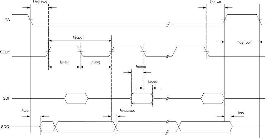
6.6 Timing Requirements: AC SPI Data Interface
Typical values stated where TA = 25°C and VBAT = 22 V, Min/Max values stated where TA = –40°C to +105°C andVBAT = 7.2 V to 27 V (unless otherwise noted) See Figure 1.
| MIN | NOM | MAX | UNIT | |||
|---|---|---|---|---|---|---|
| fSCLK | SCLK frequency(1) | 10 | 250 | 1000 | kHz | |
| SCLKDC | SCLK_H duty cycle, t(HIGH) / t(SCLK) or t(LOW) / t(SCLK) | 40% | 60% | |||
| tCS,LEAD | CS_H lead time, CS_H low to clock | 50 | SCLK/2 | ns | ||
| tCS,LAG | CS_H lag time. Last clock to CS_H high | 10 | SCLK/2 | ns | ||
| tCS,DLY | CS_H high to CS_H low (inter-packet delay requirement) | 3 | µs | |||
| tACC | CS_H access time(2): CS_H low to SDO_H data out | 125 | 250 | ns | ||
| tDIS | CS_H disable time(2): CS_H high to SDO_H high impedance | 2.5 | 2.7 | µs | ||
| tSU,SDI | SDI_H input-data setup time | 15 | ns | |||
| tHD,SDI | SDI_H input-data hold time | 10 | ns | |||
| tVALID,SDO | SDO_H output-data valid time SCLK_H edge to SDO_H valid |
CL ≤ 20 pF | 75 | 110 | ns | |
6.7 Vertical Communications Bus
Typical values stated where TA = 25°C and VBAT = 22 V (unless otherwise noted)| MIN | NOM(1) | MAX | UNIT | |||
|---|---|---|---|---|---|---|
| tHV_SCLK | Propagation delay, SCLK_H to SCLK_N | HOST = 0 | 40 | ns | ||
| tVB_SCLK | Propagation delay, SCLK_S to SCLK_N | HOST = 1 | 30 | ns | ||
| tHV_CS | Propagation delay, CS_H to CS_N | HOST = 0 | 40 | ns | ||
| tVB_CS | Propagation delay, CS_S to CS_N | HOST = 1 | 30 | ns | ||
| tHV_SDI | Propagation delay, SDI_H to SDI_N | HOST = 0 | 40 | ns | ||
| tVB_SDI | Propagation delay, SDI_S to SDI_N | HOST = 1 | 30 | ns | ||
| tHV_CONV | Propagation delay, CONV_H to CONV_N | HOST = 0 | 100 | ns | ||
| tVB_CONV | Propagation delay, CONV_S to CONV_N | HOST = 1 | 30 | ns | ||
| tHV_SDO | Propagation delay, SDO_N to SDO_H | HOST = 0 | 10 | ns | ||
| tVB_SDO | Propagation delay, SDO_N to SDO_S | HOST = 1 | 40 | ns | ||
| tHV_DRDY | Propagation delay, DRDY_N to DRDY_H | HOST = 0 | 60 | ns | ||
| tVB_DRDY | Propagation delay, DRDY_N to DRDY_S | HOST = 1 | 40 | ns | ||
| tHV_FAULT | Propagation delay, FAULT_N to FAULT_H | HOST = 0 | 55 | ns | ||
| tVB_FAULT | Propagation delay, FAULT_N to FAULT_S | HOST = 1 | 30 | ns | ||
| tHV_ALERT | Propagation delay, ALERT_N to ALERT_H | HOST = 0 | 65 | ns | ||
| tVB_ALERT | Propagation delay, ALERT_N to ALERT_S | HOST = 1 | 30 | ns | ||
6.8 Typical Characteristics
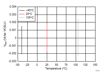
| VBAT = 27 V |
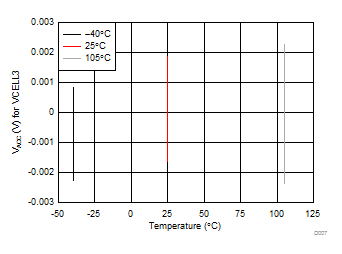
| VBAT = 27 V |
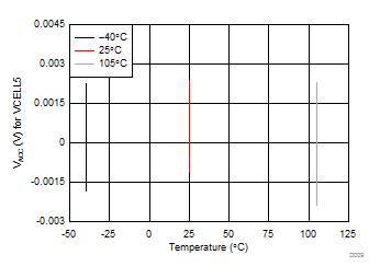
| VBAT = 27 V |
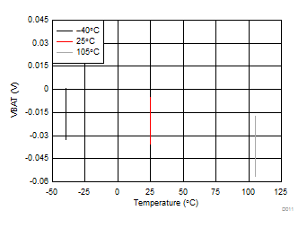
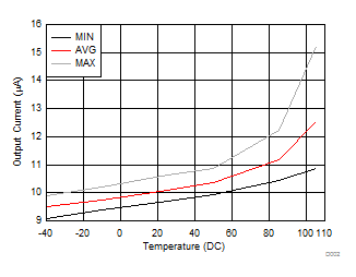
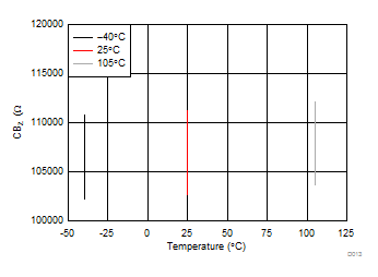
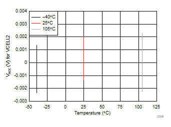
| VBAT = 27 V |
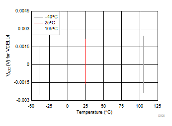
| VBAT = 27 V |
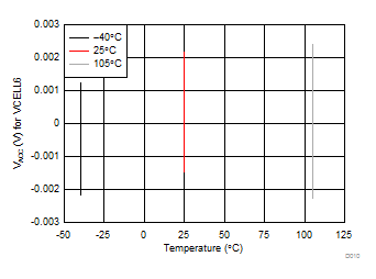
| VBAT = 27 V |
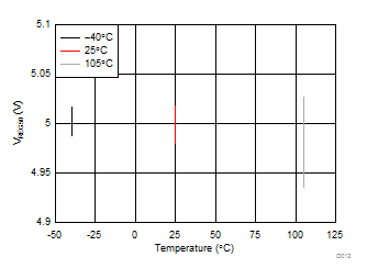
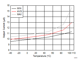
7 Detailed Description
7.1 Overview
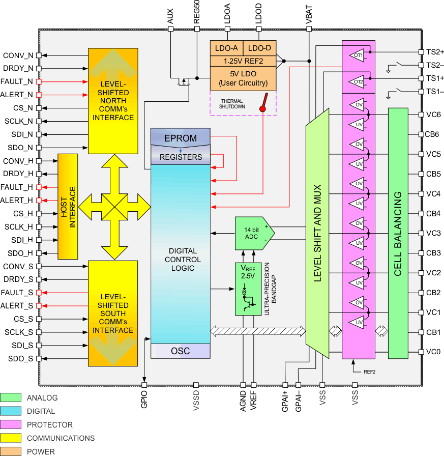
The bq76PL536A-Q1 is a 3-to-6 series Lithium-ion battery monitor, secondary protector and analog front end (AFE) that can be stacked vertically to monitor up to 192 cells without the need for additional isolation components between ICs.
This device incorporates a precision analog-to-digital converter (ADC); independent cell voltage and temperature protection; cell balancing, and precision 5-V regulator to power user circuitry. The bq76PL536A-Q1 additionally provides full (secondary) protection for overvoltage, undervoltage, and overtemperature conditions.
7.2 Functional Block Diagram
7.3 Feature Description
7.3.1 Analog-to-Digital Conversion (ADC)
7.3.1.1 General Features
The integrated 14-bit (unsigned) high-speed successive approximation register (SAR) analog-to-digital converter uses an integrated band-gap reference voltage (VREF) for the cell and brick measurements. The ADC has a front-end multiplexer for nine inputs – six cells, two temperature sensors, and one general-purpose analog input (GPAI). The GPAI input can further be multiplexed to measure the brick voltage between the BATx pin and VSS or the voltage between the GPAI+ and GPAI– pins.
The ADC and reference are factory trimmed to compensate for gain, offset, and temperature-induced errors for all inputs. The measurement result is not allowed to roll over due to offset error at the top and bottom of the range. For example, a reading near zero does not underflow to 0x03ff due to offset error and vice-versa.
The converter returns 14 valid unsigned magnitude bits in the following format:
<00xxxxxx xxxxxxxx>
Each word is returned in big-endian format in a register pair consisting of two adjacent 8-bit registers. The MSB of the word is located in the lower-address register of the pair, that is, data for cell 1 is returned in registers 0x03 and 0x04 as 00xxxxxx xxxxxxxxb.
7.3.1.2 3-to-6 Series Cell Configuration
When fewer than 6 cells are used, the most-positive cell voltage of the series string should be connected to the BAT1/BAT2 pins, through the RC input network shown in the Typical Application section. Unused VCx inputs should be connected to the next VCx input down until an input connected to a cell is reached – that is, in a four cell stack, VC6 connects to VC5, which connects to VC4 (Figure 13).
The internal multiplexer control can be set to scan only the inputs which are connected to cells, thereby speeding up conversions slightly. The multiplexer is controlled by the ADC_CONTROL[CN2:0] bits.
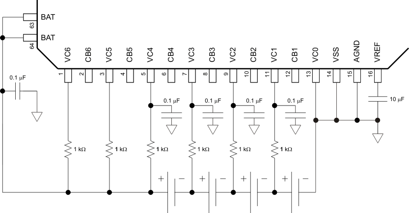 Figure 13. Connecting < 6 Cells (4 Shown)
7.3.1.3 Cell Voltage Measurements
Use the following formula (all values are in decimal) to convert the returned cell measurement value to a dc voltage (in mV).
Example:
Cell_1 == 3.35 V (3350 mV);
After conversion, REG_03 == 0x22; REG_04 == 0x4d
0x22 × 0x100 + 0x4d = 0x224d (8781.)
8781 × 6250 / 16,383 = 3349.89 mV ≈ 3.35 V
7.3.1.4 GPAI or VBAT Measurements
The bq76PL536A-Q1 features a differential input to the ADC from two external pins, GPAI+ and GPAI–. The ADC GPAI result register can be configured (via the FUNCTION_CONFIG[GPAI_SRC] to provide a measurement of the voltage on these two pins, or of the brick voltage present between the BATx pins and VC0.
In the bq76PL536A-Q1 device, the VBAT measurement is taken from the BATx pin to the VC0 pin, and is a separate input to the ADC mux. Because this is a separate input to the ADC, certain common system faults, such as a broken cell wire, can be easily detected using the bq76PL536A-Q1 and simple firmware techniques.
The GPAI measurement can be configured to use one of two references via FUNCTION_CONFIG[GPAI_REF]. Either the internal bandgap (VREF) or REG50 can be selected. When REG50 is selected, the ADC returns a ratio of the voltage at the inputs and REG50, removing the need for compensation of the REG50 voltage accuracy or drift when used as a source to excite the sensor. When the device is configured to measure VBAT (FUNCTION_CONFIG[GPAI_SRC] = 1), the device selects VREF automatically and ignores the FUNCTION_CONFIG[GPAI_REF] setting.
7.3.1.4.1 Converting GPAI Result to Voltage
To convert the returned GPAI measurement value to a voltage using the internal band-gap reference (FUNCTION_CONFIG[GPAI_REF] = 1), the following formula is used.
where
- FUNCTION_CONFIG[] = 0100 xxxxb
Example:
The voltage connected to the GPAI inputs == 1.25 V;
After conversion, REG_01 == 0x20; REG_02 == 0x00
0x20 × 0x100 + 0x00 = 0x2000 (8192.)
8192 × 2500 / 16,383 = 1250 mV
7.3.1.4.2 Converting VBAT Result to Voltage
To convert the returned VBAT measurement value to a voltage, the following formula is used.
where
- FUNCTION_CONFIG[] = 0101 xxxxb
Example:
The sum of the series cells connected to VC6–VC0 == 20.295 V;
After conversion, REG_01 == 0x26; REG_02 == 0xf7
0x26 × 0x100 + 0xf7 = 0x26f7 (9975.)
9975 × 33.333 / 16,383 = 20.295 V
7.3.1.5 Temperature Measurement
The bq76PL536A-Q1 can measure the voltage TS1+, TS1– and TS2+, TS2– differential inputs using the ADC. An external thermistor/resistor divider network typically drives these inputs. The TSn inputs use the REG50 output divided down and internally connected as the ADC reference during conversions. This produces a ratiometric result and eliminates the need for compensation or correction of the REG50 voltage drift when used to drive the temperature sensors. The REG50 reference allows an approximate 2.5-V full-scale input at the TSn inputs. The final reading is limited between 0 and 16,383, corresponding to an external ratio of 0 to 0.5.
Two control bits are required for the ADC to convert the TSn input voltages successfully. ADC_CONTROL[TSn] is set to cause the ADC to convert the TSn channel on the next requested conversion cycle. IO_CONTROL[TSn] is set to cause the FET switch connecting the TSn– input to VSS to close, completing the circuit of the voltage divider. The IO_CONTROL[] bits should only be set as needed to conserve power; at high temperatures, thermistor excitation current may be relatively high.
7.3.1.5.1 External Temperature Sensor Support (TS1+, TS1–, TS2+, and TS2–)
The device is intended for use with a nominal 10 kΩ at 25ºC NTC external thermistor (AT103 equivalent) such as the Panasonic ERT-J1VG103FA, a 1% device. A suitable external resistor-capacitor network should be connected to position the response of the thermistor within the range of interest. This is typically RT= 1.47 kΩ and RB = 1.82 kΩ (1%) as shown in Figure 14. A parallel bypass capacitor in the range 1 nF to 47 nF placed across the thermistor should be added to reduce noise coupled into the measurement system. The response time delay created by this network should be considered when enabling the respective TS input prior to conversion and setting the OT delay timer. See Figure 14 for details.
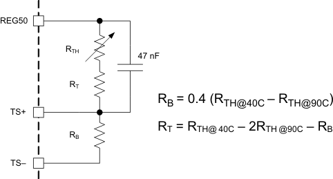 Figure 14. Thermistor Connection
7.3.1.5.2 Converting TSn Result to Voltage (Ratio)
To convert the returned TSn measurement value to a ratio, RTS = VTS:REG50, the following formulas are used. The setting FUNCTION_CONFIG[] = 0100 xxxxb is assumed. Note that the offset and gain correction are slightly different for each channel.
Example:
The voltage connected to the TS1 inputs (TS1+ – TS1–) == 0.661 V; VREG50 ≈ 5 V nominal
After conversion, REGMSB == 0x11; REGLSB == 0x16
ACTUAL_COUNT = 0x11 × 0x100 + 0x16 = 0x1116 (4374.)
(4374 + 2) / 33,046 = 0.1324 (ratio of TSn inputs to REG50)
0.1324 × REG50 = 0.662 V
7.3.1.6 ADC Band-Gap Voltage Reference
The ADC and protection subsystems use separate and independent internal voltage references. The ADC band gap (VREF) is nominally 2.5 V. The reference is temperature-compensated and stable.
The internal reference is brought out to the VREF pin for bypassing. A high quality 10-μF capacitor should be connected between the VREF and AGND pins, in very close physical proximity to the device pins, using short track lengths to minimize the effects of track inductance on signal quality. The AGND pin should be connected to VSS. Device VSS connections should be brought to a single point close to the IC to minimize layout-induced errors. The device tab should also be connected to this point, and is a convenient common VSS location. The internal VREF should not be used externally to the device by user circuits.
7.3.1.7 Conversion Control
7.3.1.7.1 Convert Start
Two methods are available to start a conversion cycle. The CONV_H pin may be asserted, or firmware may set the CONVERT_CTRL[CONV] bit.
7.3.1.7.1.1 Hardware Start
A single interface pin (CONV_H) is used for conversion-start control by the host. A conversion cycle is started by a hardware signal when CONV_H is transitioned low-to-high by the host. The host should hold this state until the conversion cycle is complete to avoid erroneous edges causing a conversion start when the present conversion is not complete. The signal is simultaneously sent to the higher device in the stack by the assertion of the CONV_N signal. The bq76PL536A-Q1 automatically sequences through the series of measurements enabled via the ADC_CONTROL[] register after a convert-start signal is received from either the register bit or the hardware pin.
If the CONV_H pin is not used in the design, this pin must be maintained in a default low state (approximately 0 V) to allow use of the ADC_CONVERT[CONV] bit to trigger ADC conversions. If the CONV pin is kept high, the ADC_CONVERT[CONV] bit does not function, and device current consumption is increased by the signaling current, approximately 900 µA. If the CONV_H pin is not used by the user’s design, the pin may be left floating; the internal current sink to VSS maintains proper bias.
7.3.1.7.1.2 Firmware Start
The CONVERT_CTRL[CONV] bit is also used to initiate a conversion by writing a 1 to the bit, which automatically resets at the end of a conversion cycle. The bit may only be written to 1; the IC always resets the bit to 0. The BROADCAST form of packet is recommended to start all device conversions simultaneously.
NOTE
For the designer: The external CONV_H (CONV_S) pin must be held in the de-asserted (=0) state to allow the CONV register bit to initiate conversions. An internal pulldown is provided on the pin to maintain this state.
7.3.1.7.2 Data Ready
The bq76PL536A-Q1 signals that data is ready when the last conversion data has been stored to the associated data result register by asserting the DRDY_S pin (DRDY_H if HOST = 0) if the DRDY_N pin is also asserted
(Figure 15). DRDY_S (DRDY_H) signals are cleared on the next conversion start.
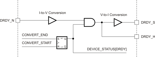 Figure 15. Data-Ready Logic
7.3.1.7.3 ADC Channel Selection
The ADC_CONTROL register can be configured as follows:
Table 1. ADC_CONTROL Register Configuration
| MEASUREMENT | ADC_CONTROL |
|---|---|
| VCELL1 | CELL_SEL = 0x00 |
| VCELL1, VCELL2 | CELL_SEL = 0x01 |
| VCELL1, VCELL2, VCELL3 | CELL_SEL = 0x02 |
| VCELL1, VCELL2, VCELL3, VCELL4 | CELL_SEL = 0x03 |
| VCELL1, VCELL2, VCELL3, VCELL4, VCELL5 | CELL_SEL = 0x04 |
| VCELL1, VCELL2, VCELL3, VCELL4, VCELL5, VCELL6 | CELL_SEL = 0x05 |
| External thermistor input 1 | TS1 = 1 |
| External thermistor input 2 | TS2 = 1 |
| General-purpose analog input | GPAI = 1 |
7.3.1.7.4 Conversion Time Control
The ADC conversion time is fixed at approximately 6 µs per converted channel, plus 6 µs overhead at the start of the conversion. Total conversion time (µs) is approximately 6 × num_channels + 6.
7.3.1.7.5 Automatic Versus Manual Control
The ADC_CONTROL[ADC_ON] bit controls powering up the ADC section and the main bandgap reference. If the bit is set to 1, the internal circuits are powered on, and current consumption by the part increases. Conversions begin immediately on command. The host CPU should wait >500 µs before initiating the qfirst conversion after setting this bit.
If the ADC_ON bit is false, an additional 500 µs is required to stabilize the reference before conversions begin.
If the sampling interval (time between conversions) used is less than approximately 10 ms, manual mode should be selected to avoid shifting the voltage reference, leading to inaccuracy in the measurements.
7.3.1.8 Secondary Protection
The bq76PL536A-Q1 integrates dedicated overvoltage and undervoltage fault detection for each cell and two overtemperature fault-detection inputs for each device. The protection circuits use a separate band-gap reference from the ADC system and operate independently. The protector also uses separate I/O pins from the main communications bus, and therefore is capable of signaling faults in hardware without intervention from the host CPU.
7.3.1.8.1 Protector Functionality
When a fault state is detected, the respective fault flag in the FAULT_STATUS[] or ALERT_STATUS[] registers is set. All flags in the FAULT and ALERT registers are then ORed into the DEVICE_STATUS[] FAULT and ALERT bits. The FAULT and ALERT bits in DEVICE_STATUS[] in turn cause the hardware FAULT_S or ALERT_S pin to be set. The bits in DEVICE_STATUS[] and the hardware pins are latched until reset by the host via SPI command, ensuring that the host CPU does not miss an event.
A separate timer is provided for each fault source (cell overvoltage, cell undervoltage, overtemperature) to prevent false alarms. Each timer is programmable from 100 µs to more than 3 s. The timers may also be disabled, which causes fault conditions to be sensed immediately and not latched.
The clearing of the FAULT or ALERT flag (and pin) occurs when the respective flag is written to a 1, which also restarts the respective fault timer. This also clears the FAULT_S (_H) or ALERT_S (_H) pin. If the actual fault remains present, the FAULT (ALERT) pin is again asserted at the expiration of the timer. This cycle repeats until the cause of the fault is removed.
On exit from the SLEEP state, the COV, CUV, and OT fault comparators are disabled for approximately 200 µs to allow internal circuitry to stabilize and prevent false error condition detection.
7.3.1.8.1.1 Using the Protector Functions With 3–5 Cells
The OV/UV condition can be ignored for unused channels by setting the FUNCTION_CONFIG[CNx] bits to the maximum number of cells connected to the device. If fewer than 6 cells are configured, the corresponding OV/UV faults are ignored. For example, if the FUNCTION_CONFIG[] bits are set to xxxx 1000, then the OV/UV comparators are disabled for cells 5 and 6. Correct setting of this register prevents spurious false alarms.
7.3.1.9 Cell Overvoltage Fault Detection (COV)
When the voltage across a cell exceeds the programmed COV threshold for a period of time greater than set in the COV timer (COVT), the COV_FAULT[] flag for that cell is set (Figure 16). The bits in COV_FAULT[] are then ORed into the FAULT[COV] flag, which is then ORed into the DEVICE_STATUS[FAULT] flag, which causes the FAULT_S (_H) pin also to be asserted. The COV flag is latched unless COVT is programmed to 0, in which case the flag follows the fault condition. Care should be taken when using this setting to avoid chatter of the fault status. To reset the FAULT flag, first remove the source of the fault (for example, the overvoltage condition) and then write a 1 to FAULT[COV], followed by a 0 to FAULT[COV]. See (Figure 16) for details.
The voltage trip point is set in the CONFIG_COV register. Set points are spaced every 50 mV. Hysteresis is provided to avoid chatter of the fault sensing. The filter delay time is set in the CONFIG_COVT[] register to prevent false alarms. A start-up deglitch circuit is applied to the timers to prevent false triggering. The deglitch time is 0–50 µs, and introduces a small error in the timing for short times. For both COVT and CUVT, this can cause an error greater than the 10% maximum specified for delays < 500 µs.
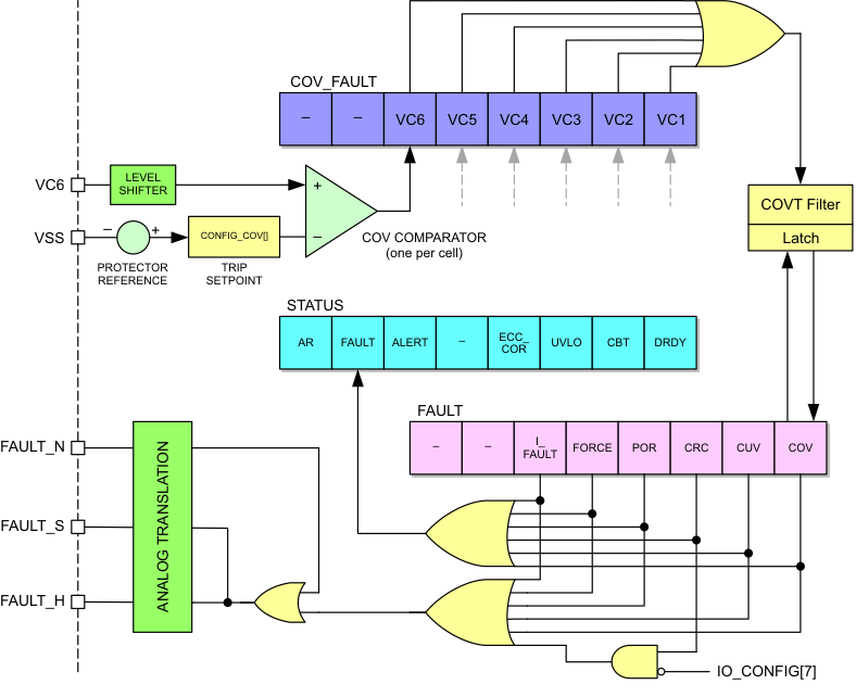 Figure 16. COV FAULT Simplified Logic Tree
7.3.1.10 Cell Undervoltage Fault Detection (CUV)
Cell undervoltage detection operates in a similar manner to the COV protection. When the voltage across a cell falls below the programmed CUV threshold (CONFIG_CUV[]) for a period of time greater than CUVT (CONFIG_CUVT[]), the CUV_FAULT[] flag for that cell is set. The bits in CUV_FAULT[] are then ORed into the FAULT[CUV] flag, which is then ORed into the DEVICE_STATUS[FAULT] flag, which causes the FAULT_S (_H) pin also to be asserted. The CUV flag is latched unless CUVT is programmed to 0, in which case the flag follows the fault condition. Care should be taken when using this setting to avoid chatter of the fault status. To reset the FAULT flag, first remove the source of the fault (for example, the overvoltage condition) and then write a 1 to FAULT[CUV], followed by a 0 to FAULT[CUV].
7.3.1.11 Overtemperature Detection
When the temperature input TS1 or TS2 exceeds the programmed OT1 or OT2 threshold (CONFIG_OT[]) for a period of time greater than OTT (CONFIG_OTT[]) the ALERT_STATUS[OT1, OT2] flag is set (Figure 17). The ALERT[] flags are then ORed into the DEVICE_STATUS[ALERT] flag, and the ALERT_S (_H) pin is also asserted. The OT flag is latched unless OTT is programmed to 0, in which case the flag follows the fault condition. Care should be taken when using this setting to avoid chatter of the fault status. To reset the FAULT flag, first remove the source of the alert (for example, the overtemperature condition) and then write a 1 to ALERT[OTn], followed by a 0 to FAULT[OTn].
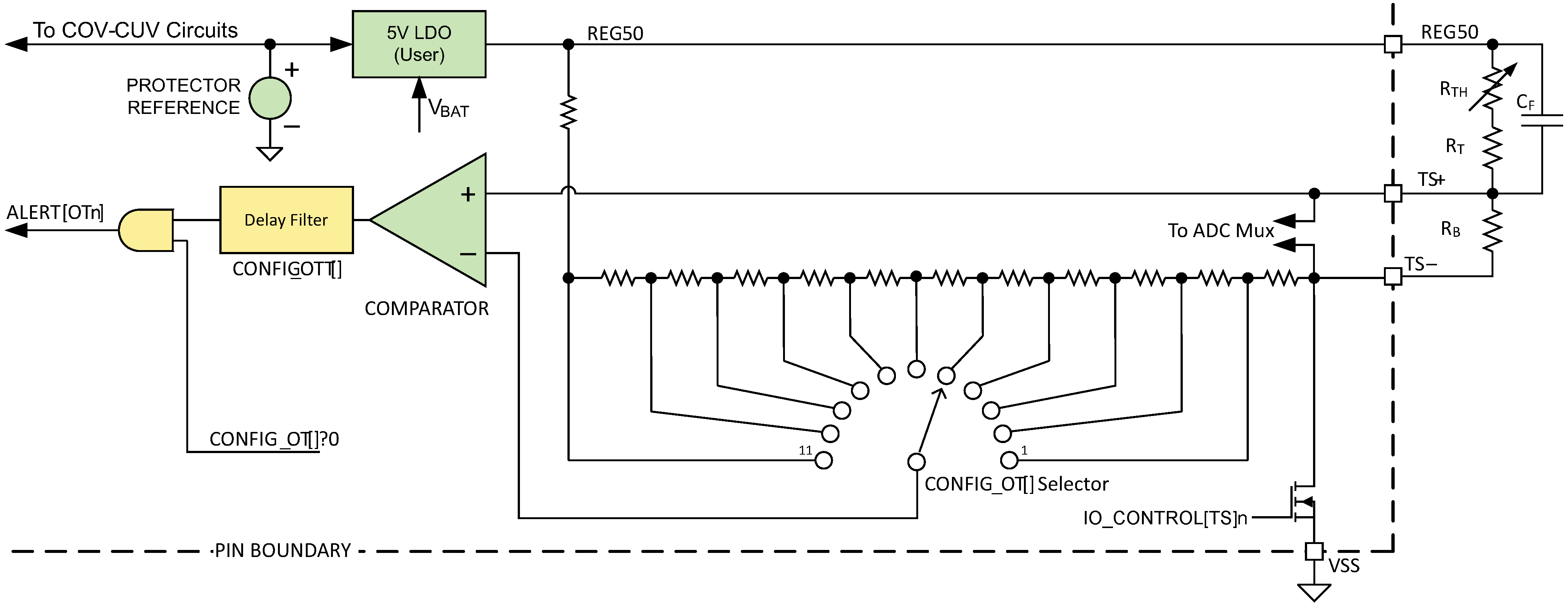 Figure 17. Simplified Overtemperature Detection Schematic
As shown in Figure 17, the OT thresholds are detectable in 11 steps representing approximately 5°C divisions when a thermistor and gain/offset setting resistors are chosen using the formula in the External Temperature Sensor Support (TS1+, TS1– and TS2+, TS2–) section. A DISABLED setting is also available. This results in an adjustment range from approximately 40°C to 90°C, but the range center can be moved by modifying the RT value. The steps are spaced in a non-linear fashion to correspond to typical thermistor response curves. Typical accuracy of a few degrees C or better can be achieved (with no additional calibration requirements) by careful selection of the thermistor and resistors.
Each input sensor can be adjusted independently via separate registers CONFIG_OT1[] and CONFIG_OT2[]. The two temperature set points share a common filter delay set in the CONFIG_OTT[] register. A setting of 0 in the CONFIG_OTT[] register causes the fault sensing to be both instantaneous and not latched. All other settings provide a latched ALERT state.
7.3.1.11.1 Ratiometric Sensing
The OT protector circuits use ratiometric inputs to sense fault conditions. The REG50 output is applied internally to the divider, which forms the reference voltages used by the comparator circuit. The REG50 output is also used externally as the excitation source for the temperature sensor. This allows the REG50 output to vary over time or temperature (within data-sheet limits) and have virtually no effect on the correct operation of the circuit. Any change seen by the sensor is also seen by the divider, and therefore, changes proportionally. Although representing the trip set points as voltages is valid, if you assume that REG50 is at exactly 5 V, in practice this is not the case. In Table 2, the correct ratios [RB/(RB + RT + RTH)] are shown, along with the equivalent voltage points when REG50 is assumed to be 5 V.
Table 2. Overtemperature Trip Set Points
| OT THRESHOLDS | |||||
|---|---|---|---|---|---|
| CONFIG_OT | TNOM °C(1) | VTS RATIO SET | VTS RATIO CLEAR | VSET(2) | VCLEAR(2) |
| 0 | Disabled | Disabled | Disabled | Disabled | Disabled |
| 1 | 40 | 0.2000 | 0.1766 | 1.000 | 0.883 |
| 2 | 45 | 0.2244 | 0.2000 | 1.122 | 1.000 |
| 3 | 50 | 0.2488 | 0.2270 | 1.244 | 1.135 |
| 4 | 55 | 0.2712 | 0.2498 | 1.356 | 1.249 |
| 5 | 60 | 0.2956 | 0.2750 | 1.478 | 1.375 |
| 6 | 65 | 0.3156 | 0.2956 | 1.578 | 1.478 |
| 7 | 70 | 0.3356 | 0.3162 | 1.678 | 1.581 |
| 8 | 75 | 0.3556 | 0.3368 | 1.778 | 1.684 |
| 9 | 80 | 0.3712 | 0.3528 | 1.856 | 1.764 |
| 10 | 85 | 0.3866 | 0.3688 | 1.933 | 1.844 |
| 11 | 90 | 0.4000 | 0.3824 | 2.000 | 1.912 |
7.3.1.11.2 Thermistor Power
To minimize power consumption, the thermistors are not powered ON by default. Two bits are provided in IO_CONTROL[] to control powering the thermistors, TS1 and TS2. The TSn– input is only connected to VSS when the corresponding bit is set. The user firmware must set these bits to 1 to enable both temperature measurement and the secondary protector functions. When the thermistor functions are not in use, the bits may be programmed to 0 to remove current through the thermistor circuits.
7.3.1.11.3 Thermistor Input Conditioning
A filter capacitor is recommended to minimize noise in to the ADC and protector. The designer should insure that the filter capacitor has sufficient time to charge before reading the thermistors. The CONFIG_OTT[] value should also be set to > 5t, the time delay introduced by the RC network comprising CF, RTH, RT, and RB, to avoid false triggering of the PROTECTOR function and ALERT signal when the TS1 and/or TS2 bits are set to 1 and the inputs enabled.
On exit from the SLEEP state, the OT fault comparators are disabled for approximately 200 µs to allow internal circuitry to stabilize and prevent false error-condition detection.
7.3.1.12 Fault and Alert Behavior
When the FAULT_N pin is asserted by the next higher bq76PL536A-Q1 in the stack, then the FAULT_S is also asserted, thereby passing the signal down the array of stacked devices if they are present. FAULT_N should always be connected to the FAULT_S of the next higher device in the stack. If no higher device exists, it should be tied to VBAT of this bq76PL536A-Q1, either directly or via a pull-up resistor from approximately 10 kΩ to 1 MΩ. The FAULT_x pins are active-high and current flows when asserted. The ALERT_x pins behave in a similar manner. If the FAULT_N pin of the base device (HSEL = 0) becomes asserted, it asserts its FAULT_H signal to the host microcontroller. This signal chain may be used to create an interrupt to the CPU or drive other compatible logic or I/O directly. See Table 3 for further details.
Table 3. Fault Detection Summary
| FAULT | DETECTION | SIGNALING | |||
|---|---|---|---|---|---|
| PIN | DEVICE_STATUS BIT SET |
X_STATUS BIT SET | |||
| HSEL = 1 | HSEL = 0 | ||||
| EPROM double bit error | ECC logic fault detected | FAULT_S | FAULT_H | FAULT | FAULT_STATUS[I_FAULT] |
| FORCE | User set FORCE bit | FAULT_S | FAULT_H | FAULT | FAULT_STATUS[FORCE] |
| POR | Power-on reset occurred | FAULT_S | FAULT_H | FAULT | FAULT_STATUS[POR] |
| CRC(1) | CRC fail on received packet | FAULT_S | FAULT_H | FAULT | FAULT_STATUS[CRC] |
| CUV | VCx < VUV for tUV | FAULT_S | FAULT_H | FAULT | FAULT_STATUS[CUV] |
| COV | VCx > VOV for tOV | FAULT_S | FAULT_H | FAULT | FAULT_STATUS[COV] |
| AR | Address ≠ (0x01→ 0x3e) | ALERT_S | ALERT_H | ALERT | ALERT_STATUS[AR] |
| Protected-register parity error | Parity not even in protected register | ALERT_S | ALERT_H | ALERT | ALERT_STATUS[PARITY] |
| EPROM single-bit error | ECC logic fault detected and corrected | ALERT_S | ALERT_H | ALERT | ALERT_STATUS[ECC_COR] |
| FORCE | User set FORCE bit | ALERT_S | ALERT_H | ALERT | ALERT_STATUS[FORCE] |
| Thermal shutdown | Die temperature ≥ TSDTHRESHOLD | ALERT_S | ALERT_H | ALERT | ALERT_STATUS[TSD] |
| SLEEP | IC exited SLEEP mode | ALERT_S | ALERT_H | ALERT | ALERT_STATUS[SLEEP] |
| OT2 | VTS2 > VOT for tOT | ALERT_S | ALERT_H | ALERT | ALERT_STATUS[OT2] |
| OT1 | VTS1 > VOT for tOT | ALERT_S | ALERT_H | ALERT | ALERT_STATUS[OT1] |
7.3.1.12.1 Fault Recovery Procedure
When any error flag in DEVICE_STATUS[], FAULT_STATUS[], or ALERT_STATUS[] is set and latched, the state can only be cleared by host communication via SPI. Writing to the respective FAULT_STATUS or ALERT_STATUS register bit with a 1 clears the latch for that bit. The exceptions are the two FORCE bits, which are cleared by writing a 0 to the bit.
The FAULT_STATUS[] and ALERT_STATUS[] register bits are read-only, with the exception of the FORCE bit, which may be directly written to either a 1 or 0.
7.3.1.13 Secondary Protector Built-In Self-Test Features
The secondary protector functions have built-in test for verifying the connections through the signal chain of ICs in the stack back to the host CPU. This verifies the wiring, connections, and signal path through the ICs by forcing a current through the signal path.
To implement this feature, host firmware should set the FAULT[FORCE] or ALERT[FORCE] bit in the top-most device in the stack. The device asserts the associated pin on the South interface, and it propagates down the stack, back to the base device. The base device in turn asserts the FAULT_H (ALERT_H) pin to the host, allowing the host to check for the received signal and thereby verify correct operation.
7.3.2 Cell Balancing
The bq76PL536A-Q1 has six dedicated outputs (CB1…CB6) that can be used to control external N-FETs as part of a cell balancing system. The implementation of appropriate algorithms is controlled by the system host. The CB_CTRL[CBAL1–6] bits control the state of each of the outputs. The outputs are copied from the bit state of the CB_CTRL register, that is, a 1 in this register activates the external balance FET by placing a high on the associated pin.
The CBx pins switch between approximately the positive and negative voltages of the cell across which the external FET is connected. This allows the use of a small, low-cost N-FET in series with a power resistor to provide cell balancing.
7.3.2.1 Cell Balance Control Safety Timer
The CBx outputs are cleared when the internal safety timer expires. The internal safety timer (CB_TIME) value is programmed in units of seconds or minutes (range set by CB_CTRL bit 7) with an accuracy of ±10%.
The timer begins when any CB_CTRL bit changes from 0 to 1. The timer is reset if all CB_CTRL bits are modified by the host from 1 to 0, or by expiration of the timing period. The timing begins counting the programmed period from start each time the CB_CTRL[] register is programmed from a zero to a non-zero value in the lower six bits. In the example, if the CB_TIME[] is set for 30 s, then one or more bits are set in the CB_CTRL[] register to balance the corresponding cells; then after 10 s, the user firmware sets CB_CTRL[] to 0x00, takes a measurement, and then reprograms CB_CTRL[] with the same or new bit pattern and the timer begins counting 30 s again before expiring and disabling balancing. This restart occurs each time the CB_CTRL bits are set to a non-zero value. If this is done at a greater rate than the balancing period for which timer CB_TIME[] is set, balancing is effectively never disabled – until the timer is either allowed to expire without changing the CB_CTRL[] register to a non-zero value, or the CB_CTRL[] register is set to zero by the user firmware. If the CB_CTRL[] register is not manipulated from zero to non-zero while the timer is running, the timer expires as expected. Alterations of the value from a non-zero to a different non-zero value do not restart the timer (such as, from 0x02 to 0x03, and so forth).
While the timer is running, the host may set or reset any bit in the CB_CTRL[] register at any time, and the CBx output follows the bit.
The host may re-program the timer at any time. The timer must always be programmed to allow the CBx outputs to be asserted. While the timer is non-zero, the CB_CTRL[] settings are reflected at the outputs.
During periods when the timer is actively running (not expired), then DEVICE_STATUS[CBT] is set.
7.3.3 Other Features and Functions
7.3.3.1 Internal Voltage Regulators
The bq76PL536A-Q1 derives power from the BAT pin using several internal low dropout (LDO) voltage regulators. There are separate LDOs for internal analog circuits (5 V at LDOA), digital circuits (5 V at LDOD1 and LDOD2), and external, user circuits (5 V at REG50). The BAT pin should be connected to the most-positive cell input from cell 3, 4, 5, or 6, depending on the number of cells connected. Locate filter capacitors as close to the IC as possible. The internal LDOs and internal VREF should not be used to power external circuitry, with the exception that LDODx should be used to source power to any external pull-up resistors.
7.3.3.1.1 Internal 5-V Analog Supply
The internal analog supply should be bypassed at the LDOA pin with a good quality, low-ESR, 2.2-μF ceramic capacitor.
7.3.3.1.2 Internal 5-V Digital Supply
The internal digital supply should be bypassed at the LDOD1(2) pin with a good-quality, low-ESR, 2.2-μF ceramic capacitor. The two pins are connected internally and provided to enhance single-pin failure-mode fault tolerance. They should also be connected together externally.
NOTE
For the Designer: Because the LDODx inputs are pulled to approximately 7 V during programming, programming time MUST be < 50 ms.
7.3.3.1.3 Low-Dropout Regulator (REG50)
The bq76PL536A-Q1 has a low-dropout (LDO) regulator provided to power the thermistors and other external circuitry. The input for this regulator is VBAT. The output of REG50 is typically 5 V. A minimum 2.2-μF capacitor is required for stable operation. The output is internally current-limited. The output is reduced to near zero if excess current is drawn, causing die temperatures to rise to unacceptable levels.
The 2.2-µF output capacitor is required whether REG50 is used in the design or not.
REG50 is disabled in SLEEP mode, and may be turned off under thermal-shutdown conditions, and therefore should not be used as a pull-up source for terminating device pins where required.
7.3.3.1.4 Auxiliary Power Output (AUX)
The bq76PL536A-Q1 provides an approximately 1-mA auxiliary power output that is controlled via IO_CONTROL[AUX]. This output is taken directly from REG50. The current drawn from this pin must be included in the REG50 current-limit budget by the designer.
7.3.3.2 Undervoltage Lockout and Power-On Reset
The device incorporates two comparators to detect low VBAT conditions. The first detects low voltage where some device digital operations are still available. The second, (POR) detects a voltage below which device operation is not ensured.
7.3.3.2.1 UVLO
When the UVLO threshold voltage is sensed for a period ≥ UVLODELAY, the device is no longer able to make accurate analog measurements and conversions. The ADC, cell-balancing and fault-detection circuitry are disabled. The digital circuitry, including host CPU and vertical communications between ICs, is fully functional. Register contents are preserved with the exception that CB_CTRL is set to 0, and the UVLO bit is set in DEVICE_STATUS[].
7.3.3.2.2 Power-On Reset (POR)
When the POR voltage threshold or lower is sensed for a period ≥ UVLODELAY, the device is no longer able to function reliably. The device is disabled, including all fault-detection circuitry, host SPI communications, vertical communications, and so forth.
After the voltage rises above the hysteresis limit longer than the delay time, the device exits the reset state, with all registers set to default conditions. The FAULT_STATUS[POR] bit is set and latched until reset by the host. The device no longer has a valid address (DEVICE_ADDRESS[AR] = 0, ADDRESS_CONTROL[] = 0). The device should be reprogrammed with a valid address, and any registers re-written if non-default values are desired.
7.3.3.2.3 Reset Command
The bq76PL536A-Q1 can also be reset by writing the reset code (0xa5) to the RESET register. All devices respond to a broadcast RESET command regardless of their current assigned address. The result is identical to a POR with the exception that the normal POR period is reduced to several hundred microseconds.
7.3.3.3 Thermal Shutdown (TSD)
The bq76PL536A-Q1 contains an integrated thermal shutdown circuit whose sensor is located near the REG50 LDO and has a threshold of TSD. When triggered, the REG50 regulator reduces its output voltage to zero, and the ADC is turned off to conserve power. The thermal shutdown circuit has a built-in hysteresis that delays recovery until the die has cooled slightly. When the thermal shutdown is active, the DEVICE_STATUS[TSD] bit is set. The IO_CONTROL[SLEEP] and ALERT[SLEEP] bits also become set to reduce power consumption.
CAUTION
The secondary protector settings are DISABLED in the TSD state.
Temperature measurement and monitoring do not function due to loss of power if the thermistors are powered from the REG50 or AUX pins and TSD occurs. Protection-dependent schemes implemented by the designer which depend on the REG50 voltage also may not function as a result of loss of the REG50 output.
7.3.3.4 GPIO
The bq76PL536A-Q1 includes a general-purpose input/output pin controlled by the IO_CONTROL[GPIO_OUT] bit. The state of this bit is reflected on the pin. To use the pin as an input, program GPIO_OUT to a 1, and then read the IO_CONTROL[GPIO_IN] bit. A pull-up (10 kΩ–1 MΩ, typ.) is required on this pin if used as an input. If the pull-up is not included in the design, system firmware must program a 0 in IO_CONTROL[GPIO_OUT] to prevent excess current draw from the floating input. Use of a pull-up is recommended in all designs to prevent an unintentional increase in current draw.
7.3.4 Communications
7.3.4.1 SPI Communications – Device to Host
Device-to-host (D2H) mode is provided on the SPI interface pins for connection to a local host microcontroller, logic, and so forth. D2H communications operate in voltage mode as a standard SPI interface for ease of connection to the outside world from the bq76PL536A-Q1 device. Standard TTL-compatible logic levels are presented. All relevant SPI timing and performance parameters are met by this interface.
The host interface operates in SPI mode 1, where CPOL = 0 and CPHA = 1. The SPI clock is normally low; data changes on rising edges, and is sampled on the falling edge. All transfers are MSB-first.
The pins of the base IC (only) in a stack should have the SCLK_H and SDI_H pins terminated with pull-ups to minimize current draw of the part if the host ever enters a state where the pins are not driven, that is, held in the high-impedance state by the host. In non-base devices, the _H pins are forced to be all outputs driven low when the HSEL pin is high. In non-base devices, all _H pins should remain unconnected.
The CS_H has a pull-up resistor of approximately 100 kΩ. SDO_H is a 3-state output and is terminated with a weak pull-up.
NOTE
For the Designer: When VBAT is at or below the UVLO trip point voltage, the internal LDO which supplies the xxxx_H host SPI communications pins (VLODx) begins to fall out of regulation. The output high voltage on the xxxx_H pins falls off with the LDO voltage in an approximately linear manner until at the POR voltage trip point it is reduced to approximately 3.5 V. This action is not tested in production.
7.3.4.2 Device-to-Device Vertical Bus (VBUS) Interface
Device-to-device (D2D) communications makes use of a unique, current-mode interface which provides common-mode voltage isolation between successive bq76PL536A-Q1s. This vertical bus (VBUS) is found on the _N and corresponding _S pins. It provides high-speed I/O for both the SPI bus and the direct I/O pins CONV and DRDY. The current-mode interface minimizes the effects of wiring capacitance on the interface speed.
The _S (south-facing) pins connect to the next-lower device (operating at a lower potential) in the stack of bq76PL536A-Q1s. The _N (North facing) pins connect to the next-higher device. The pins cannot be swapped; _S always points South, and _N always point North. The _S and _N pins are interconnected to the pin with the same name, but opposite suffix. All pins operate within the voltages present at the BAT and VSS pins.
WARNING
Use caution; these pins may be several hundred volts above system ground, depending on their position in the stack.
NOTE
For the Designer: North (_N) pins of the top, most-positive device in the stack should be connected to the BAT1(2) pins of the device for correct operation of the string. South (_S) pins of the lowest, most-negative device in the stack should be connected to VSS of the device.
The number of devices in the vertical stack and other factors limit the maximum SCLK frequency. Each device imposes an approximately 30-ns delay on the round trip communications speed, that is, from SCLK rising (an input to all devices) to the SDO pin transitioning requires approximately 30 ns per device. The designer must add to this the delay caused by the PCB trace (in turn determined by the material and layout), any connectors in series with the connection, and any other wiring or cabling between devices in the system. To maximize speed, these other system components should be carefully selected to minimize delays and other detrimental effects on signal quality. Wiring and connectors should receive special attention to their transmission line characteristics.
Other factors, which should be considered, are clock duty cycle, clock jitter, temperature effects on clock and system components, user-selected drive level for the level-shift interface, and desired design margin.
The VBUS SPI interface is placed in a low-power mode when CS_H is not asserted on the base device.
The CS_N/S pins are asserted by a logic high on the vertical interface bus (logically inverted from CS_H). This creates a default VBUS CS condition of logic low, reducing current consumption to a minimum.
To reduce power consumption of the SPI interface to a minimum, the SCLK_H and SDI_H should be maintained at a logic low (de-asserted) while CS_H is asserted (low). Most SPI buses are operated this way by microcontrollers. The VBUS versions of these signals are not inverted from the host interface. The device also de-asserts by default the SDO_N/S pins to minimize power consumption.
7.3.4.3 Packet Formats
7.3.4.3.1 Data Read Packet
When the bq76PL536A-Q1 is selected (CS_S [CS_H for first device] is active and the bq76PL536A-Q1 has been addressed) and read request has been initiated, then the data is transmitted on the SDO_S pin to the SDO_N pin of the next device down the stack. This continues to the first device in the stack, where the data in from the SDO_N pin is transmitted to the host via the SDO_H pin. The device supplying the read data generates a CRC as the last byte sent. See Figure 18 and Figure 19 for additional information.
 Figure 18. READ Packet Format
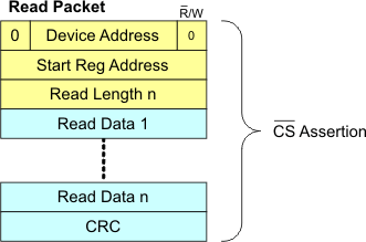 Figure 19. READ Packet Detail
7.3.4.3.2 Data Write Packet
When the bq76PL536A-Q1 is selected (CS_S is active and the bq76PL536A-Q1 has been addressed) and a write request has been initiated, the bq76PL536A-Q1 receives data through the SDI_S pin, which is connected to the SDO_N of the lower device. For the first device in the stack, the data is input to the SDI_H pin from the host, and transmitted up the stack on the SDI_S pin to the SDI_N pin of the next higher device. If enabled, the device checks the CRC, which it expects as the last byte sent. If the CRC is valid, no action is taken. If the CRC is invalid or missing, the device asserts the ALERT_S signal to the next lower device, which ripples down the stack to the ALERT_H pin on the lowest device. The host should then take action to clear the condition. See Figure 20 and Figure 21 for details.
Unused or undefined register bits should be written as zeroes.
 Figure 20. WRITE Packet Format
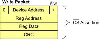 Figure 21. WRITE Packet Detail
7.3.4.3.3 Broadcast Writes
The bq76PL536A-Q1 supports broadcasting single register writes to all devices. A write to device address 0x3f is recognized by all devices on the bus with a valid address, and permits efficient simultaneous configuration of all registers in the stack of devices. This also permits synchronizing all ADC conversions by a firmware command sent to the CONVERT_CTRL[] register as an alternative to using the CONV and DRDY pins.
7.3.4.3.4 Communications Packet Structure
The bq76PL536A-Q1 has two primary communication modes via the SPI interface. These two modes enable single-byte read / write and multiple data reads. All writes are single-byte; the logical address is shifted one bit left, and the LSB = 1 for writing.
All transactions are in the form of packets comprising:
Table 4. Communication Packet Order
| BYTE | DESCRIPTION |
|---|---|
| #1 | 6-bit bq76PL536A-Q1 slave address + R/W bit 0b0xxx xxxW |
| #2 | Starting data-register offset |
| #3 | Number of data bytes to be read (n) (omitted for writes) |
| #4 to 3+n | Data bytes |
| #4+n | CRC (omit if IO_CONFIG[CRC_DIS] = 1) |
7.3.4.3.5 CRC Algorithm
The cyclic redundancy check (CRC) is a CRC-8 error-checking byte, calculated on all the message bytes (including addresses). It is identical in structure to the SMBus 2.0 packet error check (PEC), and is also known as the ATM-8 CRC. The CRC is appended to the message for all SPI packets by the device that supplied the data as the last byte in the packet (when IO_CONTROL[CRC] == 1).
Each bus transaction requires a CRC calculation by both the transmitter and receiver within each packet. The CRC is calculated in a way that conforms to the polynomial, C(x) = x8 + x2 + x1 + 1 and must be calculated in the order of the bits as received, MSB first. The CRC calculation includes all bytes in the transmission, including address, command, and data. When reading data from the device, the CRC is based on the ADDRESS + FIRST_REGISTER + LENGTH + returned_device_data[n]. The stuff-bytes used to clock out the data from the IC are not used as part of the calculation, although if the value 0x00 is used, the 0s have no effect on the CRC.
CRC verification is performed by the receiver when the CS_x line goes false, indicating the end of a packet. If the CRC verification fails, the message is ignored (discarded), the CRC failure flag is set in the FAULT_STATUS[CRC] register, and the FAULT line becomes asserted and latched until the error is read and cleared by the host.
The CRC bit returned in the FAULT_STATUS[] register reflects the last packet received, not the CRC condition of the packet reading the FAULT_STATUS contents. CRC errors should be handled at a high priority by the host controller, before writing to additional registers.
7.3.4.3.6 Data Packet Usage Examples
The bq76PL536A-Q1 can be enabled via the host to read just the specific voltage data which would require a total of 2 written bytes (chip address and R/W [#1] + first (starting) register offset [#2]) + LENGTH [#3] and 13 <null> stuff bytes (12 [n] data bytes + CRC).
The data packet can be expanded periodically to accommodate temperature and GPAI readings as well as device status as needed by changing the REGISTER_FIRST offset and LENGTH values.
7.3.4.4 Device Addressing
Each individual device, in the series stack, requires an address to allow communication with it. Each bq76PL536A-Q1 has a CS_S and CS_N that are used in assigning addresses. Once addresses have been assigned, the normal operation of the CS_N/S lines is asserted (logic high) during communications, and the appropriate bq76PL536A-Q1 in the stack responds according to the address transmitted as part of the packet (Figure 22).
When the bq76PL536A-Q1 is reset, the DEVICE_STATUS[AR] (address request) flag is cleared, the address register is set to 0x00, and ALERT_S is set and passed down the stack. In this state, where address = 0x00, the CS_N signal is forced to a de-asserted state (CS is not passed north when an address = 0). In this manner, after a reset the host is assured that a response at address 0x00 is from the first physical device in the stack. After address assignment of the current device, the host is assured that the next response at address 0x00 is from the next physical device in the stack.
Once a valid address is assigned to the device, the CS_N signal responds normally, and follows the CS_H or CS_S signal, propagating to the next device in the stack. Valid addresses are in the range 0x01 through 0x3e. 0x00 is reserved for device discovery after reset. 0x3f is reserved as a broadcast address for all devices.
NOTE
For the Designer: Broadcast messages are only received by devices with a valid address, and the next higher device. Any device with an address of 0x00 blocks messages to devices above it. A broadcast message may not be received by all devices in a stack in situations where some devices do not have a valid address.
Once the address is written, the ADDRESS_CONTROL[AR] bit is set which is copied to the DEVICE_STATUS[AR] and also ALERT_S if ALERT_N is also de-asserted. This allows the CS_N pin to follow (asserted) the CS_S pin assertions. The process of addressing can now be repeated as device ‘n’ has a new address and device n+1 has the default address of 0x00, and can be changed to its correct address in the stack.
If a device loses its address through a POR or it is replaced, then this device will be the highest logical device in the stack able to be addressed (0x00), as its CS_N will be disabled and the addressing process is required for this and higher devices.
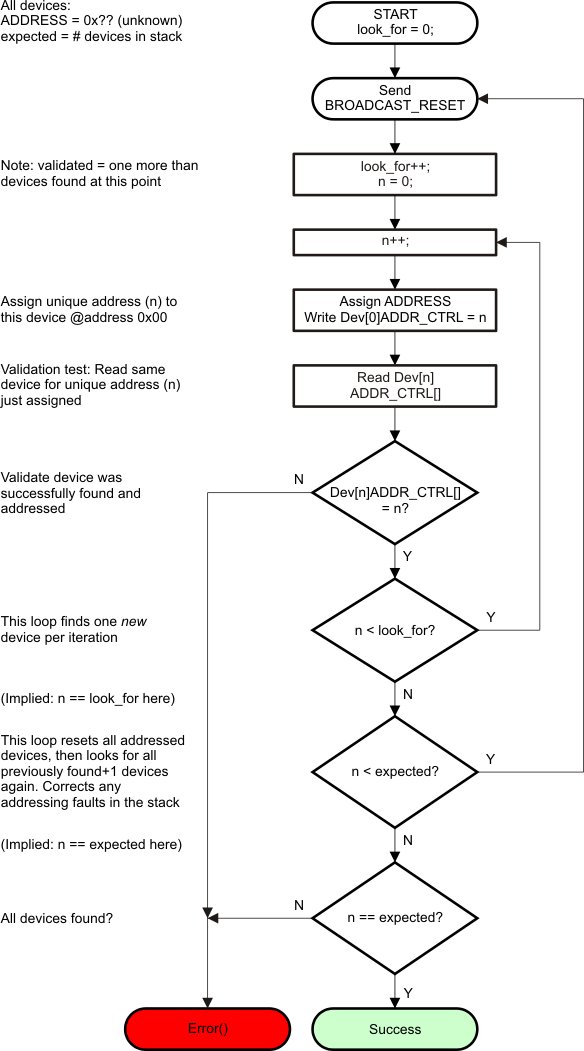 Figure 22. Address Discovery and Assignment Algorithm
7.4 Device Functional Modes
7.4.1 SLEEP Functionality
The bq76PL536A-Q1 provides the host a mechanism to put the part into a low-power sleep state by setting the IO_CONTROL[SLEEP] bit. When this bit is set/reset, the following actions occur as stated in the following paragraphs.
7.4.1.1 SLEEP State Entry (Bit Set)
If a conversion is in progress, the device waits for it to complete, then sets DRDY true (high).
The device sets the ALERT_STATUS[SLEEP] bit, which in turn causes the ALERT pin to be asserted.
The device gates off all other sources of FAULT or ALERT except ALERT[SLEEP]. The existing state of the FAULT and ALERT registers is preserved. The host should service and reset the ALERT generated by the SLEEP bit being set to minimize SLEEP state current draw by writing a 1 to ALERT[SLEEP] followed by a 0 to ALERT[SLEEP]. The ALERT North-South signal chain can draw up to approximately 1 mA of current when active, so this ALERT source should be cleared prior to the host entering the SLEEP state of its own. This signaling is provided to notify the host that the unmonitored/unprotected state is being entered.
The REG50 LDO is shut down and the output is allowed to float. The ADC, its reference, and clocks are disabled. The COV, CUV, and OT circuits are disabled, and their band-gap reference shut off.
CAUTION
The SLEEP State effectively removes protection and monitoring from the cells; the designer should take the necessary design steps and verifications to ensure the cells cannot be put into an unsafe condition by other parts of the system or usage characteristics.
IO_CONTROL[TS1:TS2] bits are not modified. The host must also set these bits to zero to minimize current draw of the thermistors themselves.
SPI communications are preserved; all registers may be read or written.
7.4.1.2 SLEEP State Exit (Bit Reset)
VREG50 operation is restored.
COV, CUV, OT circuits are re-enabled.
The ADC circuitry returns to its former state. Note that there is a warm-up delay associated with the ADC enable, the same delay as specified for enabling from a cold start.
The FAULT and ALERT registers are restored to their pre-SLEEP state. If a FAULT or ALERT condition was present prior to SLEEP, the FAULT or ALERT pin is immediately asserted.
IO_CONTROL[TS1:TS2] should be set by the host if the OT function or temperature measurement functions are desired.
7.5 Programming
7.5.1 Programming the EPROM Configuration Registers
The bq76PL536A-Q1 has a block of OTP-EPROM that is used for configuring the operation of the bq76PL536A-Q1. Programming of the EPROM should take place during pack/system manufacturing. A 7-V (VPP) pulse is required on the PROG pin. The part uses an internal window comparator to check the voltage, and times the internal pulse delivered to the EPROM array.
The user first writes the desired values to all of the equivalent Group3 protected register addresses. The desired data is written to the appropriate address by first applying 7 V to the LDOD1(2) pins. Programming then performed by writing to the EE_EN register (address 0x3f) with data 0x91. After a time period > 1500 µs, the 7 V is removed. Nominally, the voltage pulse should be applied for approximately 2–3 ms. Applying the voltage for an extended period of time may lead to device damage. The write is self-timed internally after receipt of the command. The following flow chart (Figure 23) illustrates the procedure for programming.
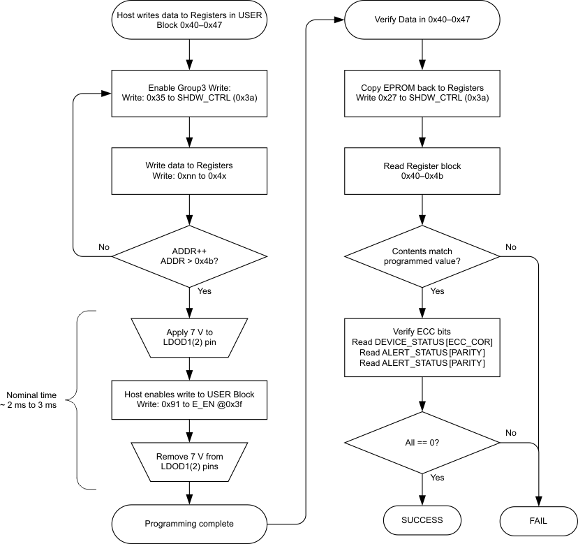 Figure 23. EPROM Programming
7.6 Register Maps
7.6.1 I/O Register Details
The bq76PL536A-Q1 has 48 addressable I/O registers. These registers provide status, control, and configuration information for the battery protection system. Reserved registers return 0x00. Unused registers should not be written to; the results are undefined. Unused or undefined bits should be written as zeroes, and will always read back as zeroes. Several types of registers are provided, details are in the following sections and tables.
7.6.2 Register Types
7.6.2.1 Read-Only (Group 1)
These registers contain the results of conversions, or device status information set by internal logic. The contents are re-initialized by a device reset as a result of either POR or the RESET command. Contents of the register are changed by either a conversion command, or when there is an internal state change (that is, a fault condition is sensed).
7.6.2.2 Read / Write (Group 2)
The Read/Write register group modifies the operations or behavior of the device, or indicates detailed status in the ALERT_STATUS[] and FAULT_STATUS[] registers (Figure 24). The contents are re-initialized by a device reset as a result of either POR or the RESET command. Contents of the register are changed either by a conversion command, or when there is an internal state change (that is, a fault condition is sensed).
Contents may also be changed by a write from the host CPU to the register. Writes may only modify a single register at a time. If CRCs are enabled, the write packet is buffered until the CRC is checked for correctness. Packets with bad CRCs are discarded without writing the value to the register, after setting the FAULT_STATUS[CRC] flag.
Unused or undefined bits in any register should be written as zeroes, and will always read back as zeroes.
 Figure 24. Register Group2 Architecture
7.6.2.3 Read / Write, Initialized From EPROM (Group3)
These registers control the device configuration and functionality. The contents of the registers are initialized from EPROM-stored constants as a result of POR, RESET command, or the RELOAD_SHADOW command. This feature ensures that the secondary protector portion of the device (COV, CUV, OT) is fully functional after any reset, without host CPU involvement. See Figure 25 for a simplified view.
These registers may only be modified by using a special, sequential-write sequence to guard against accidental changes. The value loaded from EPROM at reset (or by command) may be temporarily overwritten by using the special write sequence. The temporary value is overwritten to the programmed EPROM initialization value by the next reset or command to reload. To write to a these protected registers, first write 0x35 to SHDW_CONTROL[], immediately followed by the write to the desired register. Any intervening write cancels the special sequence.
To re-initialize the entire set of Group3 registers to the EPROM defaults, write the value 0x27 to SHDW_CONTROL[].
These registers are protected further against corruption by a ninth parity bit that is automatically updated when the register is written using even parity. If the contents of the register ever become corrupted, the bad parity causes the ALERT_STATUS[PARITY] bit to become set, alerting the host CPU of the problem.
The EPROM-stored constants are programmed by writing the values to the register(s), then applying the programming voltage to the LDODx pins, then issuing the EPROM_WRITE command to register E_EN[]. All Group3 registers are programmed simultaneously, and this operation can only be performed once to the one-time-programmable (OTP) memory cells. The process is not reversible.
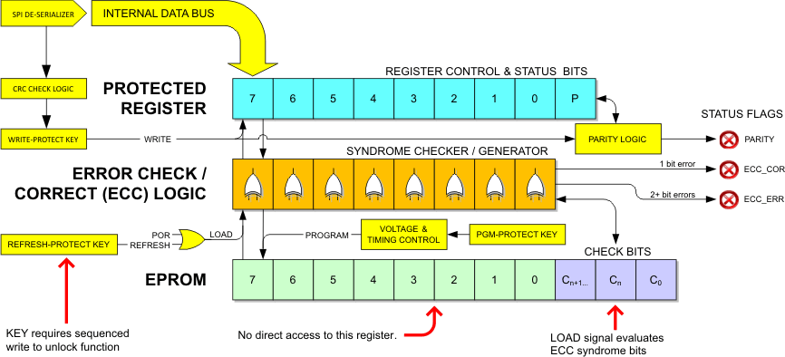 Figure 25. Protected Register Group3 Architecture, Simplified View
7.6.2.4 Error Checking and Correcting (ECC) EPROM
The EPROM used to initialize this group is also protected by error-check-and-correct (ECC) logic. The ECC bits provide a highly reliable storage solution in the presence of external disturbances. This feature cannot be disabled by user action. Implementation is fully self-contained and automatic and requires no special computations or provisioning by the user.
When the Group3 contents are permanently written to EPROM, an additional array of hidden ECC-OTP cells is also automatically programmed. The ECC logic implements a Hamming code that automatically corrects all single-bit errors in the EPROM array, and senses additional multi-bit errors. If any corrections are made, the DEVICE_STATUS[ECC_COR] flag bit is set. If any multi-bit errors are sensed, the ALERT_STATUS[ECC_ERR] flag is set. The corrective action or detection is performed anytime the contents of EPROM are loaded into the registers – POR, RESET, or by REFRESH command. Note: The ECC_COR and ECC_ERR bits may glitch during OTP-EPROM writes; this is normal. If this occurs, reset the tripped bit; it should remain cleared.
When a double-bit (uncorrectable) error is found, DEVICE_STATUS[ALERT] is set, the ALERT_S (ALERT_H for bottom stack device) line is activated, and the ALERT_STATUS[] register returns the ECC_ERR and/or I_FAULT bit = 1(true). The device may return erroneous measurement data, and/or fail to detect COV, CUV, or OT faults in this state.
EPROM bits are shipped from the factory set to 0 and must be programmed to the 1 state, as required.
Table 5. Data and Control Register Descriptions
| NAME | ADDR | GROUP | ACCESS(1) | RESET | DESCRIPTION |
|---|---|---|---|---|---|
| DEVICE_STATUS | 0x00 | 1 | R | 0 | Status register |
| GPAI | 0x01, 0x02 | 1 | R | 0 | GPAI measurement data |
| VCELL1 | 0x03, 0x04 | 1 | R | 0 | Cell 1 voltage data |
| VCELL2 | 0x05, 0x06 | 1 | R | 0 | Cell 2 voltage data |
| VCELL3 | 0x07, 0x08 | 1 | R | 0 | Cell 3 voltage data |
| VCELL4 | 0x09, 0x0a | 1 | R | 0 | Cell 4 voltage data |
| VCELL5 | 0x0b, 0x0c | 1 | R | 0 | Cell 5 voltage data |
| VCELL6 | 0x0d, 0x0e | 1 | R | 0 | Cell 6 voltage data |
| TEMPERATURE1 | 0x0f, 0x10 | 1 | R | 0 | TS1+ to TS1– differential voltage data |
| TEMPERATURE2 | 0x11, 0x12 | 1 | R | 0 | TS2+ to TS2– differential voltage data |
| RSVD | 0x13–0x1f | — | — | — | Reserved for future use |
| ALERT_STATUS | 0x20 | 2 | R/W | 0x80 | Indicates source of ALERT signal |
| FAULT_STATUS | 0x21 | 2 | R/W | 0x08 | Indicates source of FAULT signal |
| COV_FAULT | 0x22 | 1 | R | 0 | Indicates cell in OV fault state |
| CUV_FAULT | 0x23 | 1 | R | 0 | Indicates cell in UV fault state |
| PRESULT_A | 0x24 | 1 | R | 0 | Parity result of Group3 protected registers (A) |
| PRESULT_B | 0x25 | 1 | R | 0 | Parity result of Group3 protected registers (B) |
| RSVD | 0x26–0x2f | — | — | — | Reserved for future use |
| ADC_CONTROL | 0x30 | 2 | R/W | 0 | ADC measurement control |
| IO_CONTROL | 0x31 | 2 | R/W | 0 | I/O pin control |
| CB_CTRL | 0x32 | 2 | R/W | 0 | Controls the state of the cell-balancing outputs CBx |
| CB_TIME | 0x33 | 2 | R/W | 0 | Configures the CB control FETs maximum on time |
| ADC_CONVERT | 0x34 | 2 | R/W | 0 | ADC conversion start |
| RSVD | 0x35–0x39 | — | — | — | Reserved for future use |
| SHDW_CTRL | 0x3a | 2 | R/W | 0 | Controls WRITE access to Group3 registers |
| ADDRESS_CONTROL | 0x3b | 2 | R/W | 0 | Address register |
| RESET | 0x3c | 2 | W | 0 | RESET control register |
| TEST_SELECT | 0x3d | 2 | R/W | 0 | Test mode selection register |
| RSVD | 0x3e | — | — | — | Reserved for future use |
| E_EN | 0x3f | 2 | R/W | 0 | EPROM programming mode enable |
| FUNCTION_CONFIG | 0x40 | 3 | R/W | EPROM | Default configuration of device |
| IO_CONFIG | 0x41 | 3 | R/W | EPROM | I/O pin configuration |
| CONFIG_COV | 0x42 | 3 | R/W | EPROM | Overvoltage set point |
| CONFIG_COVT | 0x43 | 3 | R/W | EPROM | Overvoltage time-delay filter |
| CONFIG_CUV | 0x44 | 3 | R/W | EPROM | Undervoltage set point |
| CONFIG_CUVT | 0x45 | 3 | R/W | EPROM | Undervoltage time-delay filter |
| CONFIG_OT | 0x46 | 3 | R/W | EPROM | Overtemperature set point |
| CONFIG_OTT | 0x47 | 3 | R/W | EPROM | Overtemperature time-delay filter |
| USER1 | 0x48 | 3 | R | EPROM | User data register 1, not used by device |
| USER2 | 0x49 | 3 | R | EPROM | User data register 2, not used by device |
| USER3 | 0x4a | 3 | R | EPROM | User data register 3, not used by device |
| USER4 | 0x4b | 3 | R | EPROM | User data register 4, not used by device |
| RSVD | 0x4c–0xff | — | — | — | Reserved |
7.6.3 Register Details
7.6.3.1 DEVICE_STATUS Register (0x00)
The STATUS register provides information about the current state of the bq76PL536A-Q1.
| 7 | 6 | 5 | 4 | 3 | 2 | 1 | 0 |
| AR | FAULT | ALERT | — | ECC_COR | UVLO | CBT | DRDY |
| [7] (ADDR_RQST): | This bit is written to indicate that the ADDR[0]…[5] bits have been written to the correct address. This bit is a copy of in the ADDRESS_CONTROL[AR] bit. | |
| 0 = | Address has not been assigned | |
| 1 = | Address has been assigned | |
| [6] (FAULT): | This bit indicates that this bq76PL536A-Q1 has detected a condition causing the FAULT signal to become asserted. | |
| 0 = | No FAULT exists | |
| 1 = | A FAULT exists. Read FAULT_STATUS[] to determine the cause. | |
| [5] (ALERT): | This bit indicates that this bq76PL536A-Q1 has detected a condition causing the ALERT pin to become asserted. | |
| 0 = | No FAULT exists | |
| 1 = | An ALERT exists. Read ALERT_STATUS[] to determine the cause. | |
| [4] (not implemented) | ||
| [3] (ECC_COR): | This bit indicates a one-bit error has been detected and corrected in the EPROM. | |
| 0 = | No errors are detected in the EPROM | |
| 1 = | A one-bit (single bit) error has been detected and corrected by on-chip logic. | |
| [2] (UVLO): | This bit indicates the device VBAT has fallen below the undervoltage lockout trip point. Some device operations are not valid in this condition. | |
| 0 = | Normal operation | |
| 1 = | UVLO trip point reached, device operation is not ensured. | |
| [1] (CBT): | This bit indicates the cell balance timer is running. | |
| 0 = | The cell balance timer is has not started or has expired. | |
| 1 = | The cell balance timer is running. | |
| [0] (DRDY): | This bit indicates the data is ready to read (no conversions active). | |
| 0 = | There are conversion(s) running. | |
| 1 = | There are no conversion(s) running. | |
7.6.3.2 GPAI (0x01, 0x02) Register
The GPAI register reports the ADC measurement of GPAI+/GPAI– in units of LSBs.
Bits 15–8 are returned at address 0x01, bits 7–0 at address 0x02.
| 15 | 14 | 13 | 12 | 11 | 10 | 9 | 8 |
| GPAI[15] | GPAI [14] | GPAI [13] | GPAI [12] | GPAI [11] | GPAI [10] | GPAI [9] | GPAI [8] |
| 7 | 6 | 5 | 4 | 3 | 2 | 1 | 0 |
| GPAI [7] | GPAI [6] | GPAI [5] | GPAI [4] | GPAI [3] | GPAI [2] | GPAI [1] | GPAI [0] |
7.6.3.3 VCELLn Register (0x03…0x0e)
The VCELLn registers report the converted data for cell n, where n = 1 to 6.
Bits 15–8 are returned at odd addresses (for example, 0x03), bits 7–0 at even addresses (for example, 0x04).
| 15 | 14 | 13 | 12 | 11 | 10 | 9 | 8 |
| VCELLn[15] | VCELLn[14] | VCELLn[13] | VCELLn[12] | VCELLn[11] | VCELLn[10] | VCELLn[9] | VCELLn[8] |
| 7 | 6 | 5 | 4 | 3 | 2 | 1 | 0 |
| VCELLn[7] | VCELLn[6] | VCELLn[5] | VCELLn[4] | VCELLn[3] | VCELLn[2] | VCELLn[1] | VCELLn[0] |
7.6.3.4 TEMPERATURE1 Register (0x0f, 0x10)
The TEMPERATURE1 register reports the converted data for TS1+ to TS1–.
Bits 15–8 are returned at odd addresses (for example, 0x0f), bits 7–0 at even addresses (for example, 0x10).
| 15 | 14 | 13 | 12 | 11 | 10 | 9 | 8 |
| TEMP1[15] | TEMP1[14] | TEMP1[13] | TEMP1[12] | TEMP1[11] | TEMP1[10] | TEMP1[9] | TEMP1[8] |
| 7 | 6 | 5 | 4 | 3 | 2 | 1 | 0 |
| TEMP1[7] | TEMP1[6] | TEMP1[5] | TEMP1[4] | TEMP1[3] | TEMP1[2] | TEMP1[1] | TEMP1[0] |
7.6.3.5 TEMPERATURE2 Register (0x11, 0x12)
The TEMPERATURE2 register reports the converted data for TS2+ to TS2–.
Bits 15–8 are returned at odd addresses (for example, 0x11), bits 7–0 at even addresses (for example, 0x12).
| 15 | 14 | 13 | 12 | 11 | 10 | 9 | 8 |
| TEMP2[15] | TEMP2[14] | TEMP2[13] | TEMP2[12] | TEMP2[11] | TEMP2[10] | TEMP2[9] | TEMP2[8] |
| 7 | 6 | 5 | 4 | 3 | 2 | 1 | 0 |
| TEMP2[7] | TEMP2[6] | TEMP2[5] | TEMP2[4] | TEMP2[3] | TEMP2[2] | TEMP2[1] | TEMP2[0] |
7.6.3.6 ALERT_STATUS Register (0x20)
The ALERT_STATUS register provides information about the source of the ALERT signal. The host must clear each alert flag by writing a 1 to the bit that is set. The exception is bit 4, which may be written 1 or 0 as needed to implement self-test of the IC stack and wiring.
| 7 | 6 | 5 | 4 | 3 | 2 | 1 | 0 |
| AR | PARITY | ECC_ERR | FORCE | TSD | SLEEP | OT2 | OT1 |
| [7] (AR): | This bit indicates that the ADDR[0]…[5] bits have been written to a valid address. This bit is an inverted copy of the ADDRESS_CONTROL[AR] bit. It is not cleared until an address has been programmed in ADDRESS_CONTROL and a 1 followed by a 0 (two writes) is written to the bit. | |
| 0 = | Address has been assigned. | |
| 1 = | Address has not been assigned (default at RESET). | |
| [6] (PARITY): | This bit is used to validate the contents of the protected Group3 registers. | |
| 0 = | Group3 protected register(s) contents are valid. | |
| 1 = | Group3 protected register(s) contents are invalid. Group3 registers should be refreshed from OTP or directly written from the host. | |
| [5] (ECC_ERR): | This bit is used to validate the OTP register blocks. | |
| 0 = | No double-bit errors (a corrected one-bit error may/may not exist) | |
| 1 = | An uncorrectable error has been detected in the OTP-EPROM register bank. OTP-EPROM register(s) are not valid. | |
| [4] (FORCE): | This bit asserts the ALERT signal. It can be used to verify correct operation and connectivity of the ALERT as a part of system self-test. | |
| 0 = | De-assert ALERT (default) | |
| 1 = | Assert the ALERT signal. | |
| [3] (TSD): | This bit indicates thermal shutdown is active. | |
| 0 = | Thermal shutdown is inactive (default). | |
| 1 = | Die temperature has exceeded TSD. | |
| [2] (SLEEP): | This bit indicates SLEEP mode was activated. This bit is only set when SLEEP is first activated; no continuous ALERT or SLEEP status is indicated after the host resets the bit, even if the IO_CONTROL[SLEEP] bit remains true. (See IO_CONTROL[] register for details.) | |
| 0 = | Normal operation | |
| 1 = | SLEEP mode was activated. | |
| [1] (OT2): | This bit indicates an overtemperature fault has been detected via TS2. | |
| 0 = | Temperature is lower than or equal to the VOT2 (or input disabled by IO_CONTROL[TS2] = 0). | |
| 1 = | Temperature is higher than VOT2. | |
| [0] (OT1): | This bit indicates an overtemperature fault has been detected via TS1. | |
| 0 = | Temperature is lower than or equal to the VOT1 (or input disabled by IO_CONTROL[TS1] = 0). | |
| 1 = | Temperature is higher than VOT1. | |
7.6.3.7 FAULT_STATUS Register (0x21)
The FAULT_STATUS register provides information about the source of the FAULT signal, see Error Checking and Correcting (ECC) EPROM for more information. The host must clear each fault flag by writing a 1 to the bit that is set. The exception is bit 4, which may be written 1 or 0 as needed to implement self-test of the IC stack and wiring.
| 7 | 6 | 5 | 4 | 3 | 2 | 1 | 0 |
| — | — | I_FAULT | FORCE | POR | CRC | CUV | COV |
| [7] | Not implemented. | |
| [6] | Not implemented. | |
| [5] (I_FAULT): | The device has failed an internal register consistency check. Measurement data and protection function status may not be accurate and should not be used. | |
| 0 = | No internal register consistency check fault exists. | |
| 1 = | The internal consistency check has failed self-test. The host should attempt to reset the devices, see the RESET section. If the fault persists, the failure should be considered uncorrectable. | |
| [4] (FORCE): | This bit asserts the FAULT signal. It can be used to verify correct operation and connectivity of the FAULT line as a part of system self-test. | |
| 0 = | De-assert FAULT (default) | |
| 1 = | Assert the FAULT signal. | |
| [3] (POR): | This bit indicates a power-on reset (POR) has occurred. | |
| 0 = | No POR has occurred since this bit was last cleared by the host. | |
| 1 = | A POR has occurred. This notifies the host that default values have been loaded to Group1 and Group2 registers and OTP contents have been copied to Group3 registers. | |
| [2] (CRC): | This bit indicates a garbled packet reception by the device. | |
| 0 = | Normal errors | |
| 1 = | A CRC error was detected in the last packet received. | |
| [1] (CUV): | This bit indicates that this bq76PL536A-Q1 has detected a cell undervoltage (CUV) condition. Examine CUV_FAULT[] to determine which cell caused the ALERT. | |
| 0 = | All cells are above the CUV threshold (default). | |
| 1 = | One or more cells are below the CUV threshold. | |
| [0] (COV): | This bit indicates that this bq76PL536A-Q1 has detected a cell overvoltage (COV) condition. Examine COV_FAULT[] to determine which cell caused the FAULT. | |
| 0 = | All cells are below the COV threshold (default). | |
| 1 = | One or more cells are above the COV threshold. | |
7.6.3.8 COV_FAULT Register (0x22)
| 7 | 6 | 5 | 4 | 3 | 2 | 1 | 0 |
| — | — | OV[6] | OV[5] | OV[4] | OV[3] | OV[2] | OV[1] |
| [0..5] (OV[1]..[6]): | These bits indicate which cell caused the DEVICE_STATUS[COV] flag to be set. | |
| 0 = | Cell[n] does not have an overvoltage fault (default). | |
| 1 = | Cell[n] does have an overvoltage fault. | |
7.6.3.9 CUV_FAULT Register (0x23)
| 7 | 6 | 5 | 4 | 3 | 2 | 1 | 0 |
| — | — | UV[6] | UV[5] | UV[4] | UV[3] | UV[2] | UV[1] |
| b0..5 (UV[1]..[6]): | These bits indicate which cell caused the DEVICE_STATUS[CUV] flag to be set. | |
| 0 = | Cell[n] does not have an undervoltage fault (default). | |
| 1 = | Cell[n] does have an undervoltage fault. | |
7.6.3.10 PARITY_H Register (0x24) [PRESULT_A (R/O)]
The PRESULT_A register holds the parity result bits for the first eight Group3 protected registers.
| 7 | 6 | 5 | 4 | 3 | 2 | 1 | 0 |
| OTT | OTV | CUVT | CUVV | COVT | COVV | IO | FUNC |
7.6.3.11 PARITY_H Register (0x25) [PRESULT_B (R/O)]
The PRESULT_B register holds the parity result bits for the second eight Group3 protected registers.
| 7 | 6 | 5 | 4 | 3 | 2 | 1 | 0 |
| 0 | 0 | 0 | 0 | USER4 | USER3 | USER2 | USER1 |
7.6.3.12 ADC_CONTROL Register (0x30)
The ADC_CONTROL register controls some features of the bq76PL536A-Q1.
| 7 | 6 | 5 | 4 | 3 | 2 | 1 | 0 |
| — | ADC_ON | TS2 | TS1 | GPAI | CELL_SEL[2] | CELL_SEL[1] | CELL_SEL[0] |
| [7] Not implemented. Must be written as 0. | ||||||
| [6] (ADC_ON): | This bit forces the ADC subsystem ON. This has the effect of eliminating internal start-up and settling delays, but increases current consumption. | |||||
| 0 = | Auto mode. ADC subsystem is OFF until a conversion is requested. The ADC is turned on, a wait is applied to allow the reference to stabilize. Automatically returns to OFF state at end of requested conversion. Note that there is a start-up delay associated with turning the ADC to the ON state in this mode. | |||||
| 1 = | ADC subsystem is ON, regardless of conversion state. Power consumption is increased. | |||||
Table 6. Temperature sensor Inputs
| TS[1] | TS[0] | MEASURE T |
|---|---|---|
| 0 | 0 | None (default) |
| 0 | 1 | TS1 |
| 1 | 0 | TS2 |
| 1 | 1 | Both |
| [3] (GPAI): | This bit enables and disables the GPAI input to be measured on the next conversion-sequence start. | |||||
| 0 = | GPAI is not selected for measurement. | |||||
| 1 = | GPAI is selected for measurement. | |||||
| [2–0] (CELL_SEL): | These three bits select the series cells for voltage measurement translation on the next conversion sequence start. | |||||
Table 7. Series Cells for Voltage Measurement Translation
| CELL_SEL[2] | CELL_SEL[1] | CELL_SEL[0] | SELECTED CELL |
|---|---|---|---|
| 0 | 0 | 0 | Cell 1 only |
| 0 | 0 | 1 | Cells 1-2 |
| 0 | 1 | 0 | Cells 1-2-3 |
| 0 | 1 | 1 | Cells 1-2-3-4 |
| 1 | 0 | 0 | Cells 1-2-3-4-5 |
| 1 | 0 | 1 | Cells 1-2-3-4-5-6 |
| Other | Cell 1 only | ||
7.6.3.13 IO_CONTROL Register (0x31)
The IO_CONTROL register controls some features of the bq76PL536A-Q1 external I/O pins.
| 7 | 6 | 5 | 4 | 3 | 2 | 1 | 0 |
| AUX | GIPI_OUT | GPIO_IN | 0 | 0 | SLEEP | TS2 | TS1 |
| [7] (AUX): | Controls the state of the AUX output pin, which is internally connected to REG50. | |
| 0= | Open | |
| 1= | Connected to REG50 | |
| [6] (GPIO_OUT): | Controls the state of the open-drain GPIO output pin; the pin should be programmed to 1 to use the GPIO pin as an input. | |
| 0= | Output low | |
| 1= | Open-drain | |
| [5] (GPIO_IN): | Represents the input state of GPIO pin when used as an input. | |
| 0= | GPIO input is low. | |
| 1= | GPIO input is high. | |
| [4] Not implemented. Must be written as 0. | ||
| [3] Not implemented. Must be written as 0. | ||
| [2] (SLEEP): | Places the device in a low quiescent-current state. All CUV, COV, and OT comparators are disabled. A 1-ms delay to stabilize the reference voltage is required to exit SLEEP mode and return to active COV, CUV monitoring. | |
| 0= | ACTIVE mode | |
| 1= | SLEEP mode | |
| [1..0] (TSx): | Controls the connection of the TS1:TS2 inputs to the ADC VSS connection point. When set, the TSx(–) input is connected to VSS. These bits should be set to 0 to reduce the current draw of the system. | |
| 0= | Not connected | |
| 1= | Connected | |
7.6.3.14 CB_CTRL Register (0x32)
The CB_CTRL register determines the internal cell-balance output state.
| 7 | 6 | 5 | 4 | 3 | 2 | 1 | 0 |
| — | — | CBAL[6] | CBAL[5] | CBAL[4] | CBAL[3] | CBAL[2] | CBAL[1] |
| CB_CTRL b(n = 5 to 0) (CBAL(n + 1)): This bit determines if the CB(n) output is high or low. | ||
| 0 = | CB[n] output is low (default). | |
| 1 = | CB[n] output is high (active). | |
7.6.3.15 CB_TIME Register (0x33)
The CB_TIME register sets the maximum high (active) time for the cell balance outputs from 0 seconds to 63 minutes. When set to 0, no balancing can occur – balancing is effectively disabled.
| 7 | 6 | 5 | 4 | 3 | 2 | 1 | 0 |
| CBT[7] | — | CBT[5] | CBT[4] | CBT[3] | CBT[2] | CBT[1] | CBT[0] |
| [7] | Controls minutes/seconds counting resolution. | |
| 0 = | Seconds (default) | |
| 1 = | Minutes | |
| [5..0] | Sets the time duration as scaled by CBT.7 | |
7.6.3.16 ADC_CONVERT Register (0x34)
The CONVERT_CTRL register is used to start conversions.
| 7 | 6 | 5 | 4 | 3 | 2 | 1 | 0 |
| — | — | — | — | — | — | — | CONV |
7.6.3.17 SHDW_CTRL Register (0x3a)
The SHDW_CTRL register controls writing to Group3 protected registers. Default at RESET = 0x00.
The value 0x35 must be written to this register to allow writing to Group3 protected registers in the range 0x40–0x4f. The register always returns 0x00 on read. The register is reset to 0x00 after any successful write, including a write to non-Group3 registers. A read operation does not reset this register.
Writing the value 0x27 results in all Group3 protected registers being refreshed from OTP programmed values. The register is reset to 0x00 after the REFRESH is complete.
| 7 | 6 | 5 | 4 | 3 | 2 | 1 | 0 |
| SHDW[7] | SHDW[6] | SHDW[5] | SHDW[4] | SHDW[3] | SHDW[2] | SHDW[1] | SHDW[0] |
7.6.3.18 ADDRESS_CONTROL Register (0x3b)
The ADDRESS_CONTROL register allows the host to assign an address to the bq76PL536A-Q1 for communication. The default for this register is 0x00 at RESET.
| 7 | 6 | 5 | 4 | 3 | 2 | 1 | 0 |
| AR | 0 | ADDR[5] | ADDR[4] | ADDR[3] | ADDR[2] | ADDR[1] | ADDR[0] |
| [7] (ADDR_RQST): | This bit is written to indicate that the ADDR[0]…[5] bits have been written to the correct address. This bit is reflected in the DEVICE_STATUS[AR] bit | |
| 0 = | Address has not been assigned (default at RESET). | |
| 1 = | Address has been assigned. | |
| [5..0] (ADDR): | These bits set the device address for SPI communication. This provides to a range of addresses from 0x00 to 0x3f. Address 0x3f is reserved for broadcast messages to all connected and addressed 76PL536 devices. The default for these 6 bits is 0x00 at RESET. | |
7.6.3.19 RESET Register (0x3c)
The RESET register allows the host to reset the bq76PL536A-Q1 directly.
Writing 0xa5 causes the device to RESET. Other values are ignored.
| 7 | 6 | 5 | 4 | 3 | 2 | 1 | 0 |
| RST[7] | RST[6] | RST[5] | RST[4] | RST[3] | RST[2] | RST[1] | RST[0] |
7.6.3.20 TEST_SELECT Register (0x3d)
The TEST_SELECT places the SPI port in a special mode useful for debug.
TSEL (b7–b0) is used to place the SPI_H interface pins in a mode to support test/debug of a string of bq76PL536A-Q1 devices. 0 = normal operating mode.
When the sequence 0xa4, 0x25 ("JR") is written on subsequent write cycles, the device enters a special TEST mode useful for stack debugging. Writes to other registers between the required sequence bytes results in the partial sequence being voided; the entire sequence must be written again. POR, RESET, or writing a 0x00 to this register location exits this mode.
In this state, SPI pin SCLK and SDI become outputs and are enabled, and reflect the state of the SCLK_S, SDI_S pins of the device. SDO remains an output. This allows observation of bus traffic mid-string. The lowest device in the string should not be set to operate in this mode.
CAUTION
The user is cautioned to condition the connection to a mid- or top-string device with suitable isolation circuitry to prevent injury or damage to connected devices. Programming the most-negative device on the stack in this mode prevents further communications with the stack until POR, and may result in device destruction; this condition should be avoided.
| 7 | 6 | 5 | 4 | 3 | 2 | 1 | 0 |
| TSEL[7] | TSEL[6] | TSEL[5] | TSEL[4] | TSEL[3] | TSEL[2] | TSEL[1] | TSEL[0] |
7.6.3.21 E_EN Register (0x3f)
The E_EN register controls the access to the programming of the integrated OTP EPROM.
This register should be written the value 0x91 to permit writing the USER block of EPROM. Values other than 0x00 and 0x91 are reserved and may result in undefined operation. The next read or write of any type to the device resets (closes) the write window. If a Group3 protected write occurs, the window is closed after the write.
| 7 | 6 | 5 | 4 | 3 | 2 | 1 | 0 |
| E_EN[7] | E_EN [6] | E_EN [5] | E_EN [4] | E_EN [3] | E_EN [2] | E_EN [1] | E_EN [0] |
7.6.3.22 FUNCTION_CONFIG Register (0x40)
The FUNCTION_CONFIG sets the default configuration for special features of the device.
| 7 | 6 | 5 | 4 | 3 | 2 | 1 | 0 |
| 0 | 0 | GPAI_REF | GPAI_SRC | CN[1] | CN[0] | — | 0 |
| [7..6] (0) | Reserved | |||||
| [5] (GPAI_REF): | This bit sets the reference for the GPAI ADC measurement. | |||||
| 0 = | Internal ADC bandgap reference | |||||
| 1 = | VREG50 (ratiometric) | |||||
| [4] (GPAI_SRC): | This bit controls multiplexing of the GPAI register and determines whether the ADC mux is connected to the external GPAI inputs, or internally to the BAT1 pin. The register results are scaled automatically to match the input. | |||||
| 0 = | External GPAI inputs are converted to result in GPAI register 0x01–02. | |||||
| 1 = | BAT pin to VSS voltage is measured and reported in the GPAI register. | |||||
| [3..2] (CN[1..0]): | These two bits configure the number of series cells used. If fewer than 6 cells are configured, the corresponding OV/UV faults are ignored. For example, if the CN[x] bits are set to 10b (2), then the OV/UV comparators are ignored for cells 5 and 6. Refer to Table 8. | |||||
Table 8. Series Cells
| CN[1] | CN[0] | SERIES CELLS |
|---|---|---|
| 0 | 0 | 6 (DEFAULT) |
| 0 | 1 | 5 |
| 1 | 0 | 4 |
| 1 | 1 | 3 |
7.6.3.23 IO_CONFIG Register (0x41)
The IO_CONFIG sets the default configuration for miscellaneous I/O features of the device.
| 7 | 6 | 5 | 4 | 3 | 2 | 1 | 0 |
| CRCNOFLT | — | — | — | — | — | — | CRC_DIS |
| [7] (CRCNOFLT): | This bit enables and disables detected CRC errors asserting the FAULT pin. | |
| 0 = | CRC errors cause the FAULT[CRC] bit to be set and the FAULT pin to assert. The FAULT[CRC] bit must be reset as described in the text. | |
| 1 = | CRC errors cause the FAULT[CRC] bit to be set and the FAULT pin is not asserted. The FAULT[CRC] bit must be reset as described in the text. | |
| [0] (CRC_DIS): | This bit enables and disables the automatic generation of the CRC for the SPI communication packet. The packet size is determined by the host as part of the read request protocol. The CRC is checked at the de-assertion of the CS pin. TI recommends that this bit be changed using the broadcast address (0x3f), so that all devices in a battery stack use the same protocol. | |
| 0 = | A CRC is expected, and generated as the last byte of the packet. | |
| 1 = | A CRC is not used in communications. | |
7.6.3.24 CONFIG_COV Register (0x42)
The CONFIG_COV register determines cell-overvoltage threshold voltage.
| 7 | 6 | 5 | 4 | 3 | 2 | 1 | 0 |
| DISABLE | — | COV[5] | COV[4] | COV[3] | COV[2] | COV[1] | COV[0] |
| [7] (DISABLE): | Disables the overvoltage function when set | |
| 0 = | Overvoltage function enabled | |
| 1 = | Overvoltage function disabled | |
| [5..0] (COV[5]…[0]): | Configuration bits with corresponding voltage threshold | |
| 0x00 = 2 V; each binary increment adds 50 mV until 0x3c = 5 V. | ||
7.6.3.25 CONFIG_COVT Register (0x43)
The CONFIG_COVT register determines cell-overvoltage detection delay time.
| 7 | 6 | 5 | 4 | 3 | 2 | 1 | 0 |
| µs/ms | — | — | COVD[4] | COVD[3] | COVD[2] | COVD[1] | COVD[0] |
| [7] (µs/ms): | Determines the units of the delay time, microseconds or milliseconds | |
| 0 = | Microseconds | |
| 1 = | Milliseconds | |
| [4..0] COVD: | 0x01 = 100; each binary increment adds 100 until 0x1f = 3100 | |
| Note: | When this register is programmed to 0x00, the delay becomes 0s AND the COV state is NOT latched in the COV_FAULT[] register. In this operating mode, the overvoltage state for a cell is virtually instantaneous in the COV_FAULT[] register. This mode may cause system firmware to miss a dangerous cell overvoltage condition. | |
7.6.3.26 CONFIG_UV Register (0x44)
The CUV register determines cell-undervoltage threshold voltage.
| 7 | 6 | 5 | 4 | 3 | 2 | 1 | 0 |
| DISABLE | — | — | CUV[4] | CUV[3] | CUV[2] | CUV[1] | CUV[0] |
| [7] (DISABLE): | Disables the undervoltage function when set | |
| 0 = | Undervoltage function enabled | |
| 1 = | Undervoltage function disabled | |
| [5..0] (CUV[4]…[0]): | Configuration bits with corresponding voltage threshold 0x00 = 0.7 V; each binary increment adds 100 mV until 0x1a = 3.3 V. |
|
7.6.3.27 CONFIG_CUVT Register (0x45)
The CONFIG_CUVT register determines cell-overvoltage detection delay time.
| 7 | 6 | 5 | 4 | 3 | 2 | 1 | 0 |
| µs/ms | — | — | CUVD[4] | CUVD[3] | CUVD[2] | CUVD[1] | CUVD[0] |
| [7] (µs/ms): | Determines the units of the delay time, microseconds or milliseconds | |
| 0 = | Microseconds | |
| 1 = | Milliseconds | |
| [4..0] CUVD: | 0x01 = 100; each binary increment adds 100 until 0x1f = 3100. | |
| Note: | When this register is programmed to 0x00, the delay becomes 0 s AND the CUV state is NOT latched in the CUV_FAULT[] register. In this operating mode, the overvoltage state for a cell is virtually instantaneous in the CUV_FAULT[] register. This mode may cause system firmware to miss a dangerous cell undervoltage condition. | |
7.6.3.28 CONFIG_OT Register (0x46)
The CONFIG_OT register holds the configuration of the overtemperature thresholds for the two TS inputs.
For each respective nibble (OT1 or OT2), the value 0x0 disables this function. Other settings program a trip threshold. See the Ratiometric Sensing section for details of setting this register. Values above 0x0b are illegal and should not be used.
| 7 | 6 | 5 | 4 | 3 | 2 | 1 | 0 |
| OT2[3] | OT2[2] | OT2[1] | OT2[0] | OT1[3] | OT1[2] | OT1[1] | OT1[0] |
7.6.3.29 CONFIG_OTT Register (0x47)
The CONFIG_OTT register determines cell overtemperature detection delay time.
0x01 = 10 ms; each binary increment adds 10 ms until 0xff = 2.55 seconds.
| 7 | 6 | 5 | 4 | 3 | 2 | 1 | 0 |
| COTD[7] | COTD[6] | COTD[5] | COTD[4] | COTD[3] | COTD[2] | COTD[1] | COTD[0] |
| Note: | When this register is programmed to 0x00, the delay becomes 0 s AND the OT state is NOT latched in the ALERT_STATUS[] register. In this operating mode, the overtemperature state for a TSn input is virtually instantaneous in the register. This mode may cause system firmware to miss a dangerous overtemperature condition. |
7.6.3.30 USERx Register (0x48–0x4b) (USER1–4)
The four USER registers can be used to store user data. The part does not use these registers for any internal function. They are provided as convenient storage for user S/N, date of manufacture, and so forth.
| 7 | 6 | 5 | 4 | 3 | 2 | 1 | 0 |
| USER[7] | USER[6] | USER[5] | USER[4] | USER[3] | USER[2] | USER[1] | USER[0] |
8 Application and Implementation
NOTE
Information in the following applications sections is not part of the TI component specification, and TI does not warrant its accuracy or completeness. TI’s customers are responsible for determining suitability of components for their purposes. Customers should validate and test their design implementation to confirm system functionality.
8.1 Application Information
The bq76PL536A-Q1 is a series cell Lithium-Ion battery monitor and secondary protector for Electric Vehicles (EV), Hybrid Electric Vehicles (HEV), Uninterruptible Power Systems (UPS), E-Bike/Scooter, Large-Format Battery Systems, and so forth.
To allow for optimal performance in the end application, special consideration must be taken to ensure minimization of measurement error through proper printed circuit board (PCB) layout.
8.1.1 Anti-Aliasing Filter
An anti-aliasing filter is required for each VCn input VC6–VC1, consisting of a 1-kΩ, 1% series resistor and 100-nF capacitor. Good-quality components should be used. A 1% resistor is recommended, because the resistor creates a small error by forming a voltage divider with the input impedance of the part. The part is factory-trimmed to compensate for the error introduced by the filter.
8.1.2 Host SPI Interface Pin States
The CS_H pin is active-low. The host asserts the pin to a logic zero to initiate communications. The CS pin should remain low until the end of the current packet. When the CS_H pin is asserted, the SPI receiver and interface of the device are reset and resynchronized. This action ensures that a slave device that has lost synchronization during a previous transmission or as the result of noise on the bus does not remain permanently hung. CS_H must be driven false (high) between packets; see Timing Requirements: AC SPI Data Interface, for timing details.
8.2 Typical Application
Full-size reference schematics are available from TI on request.
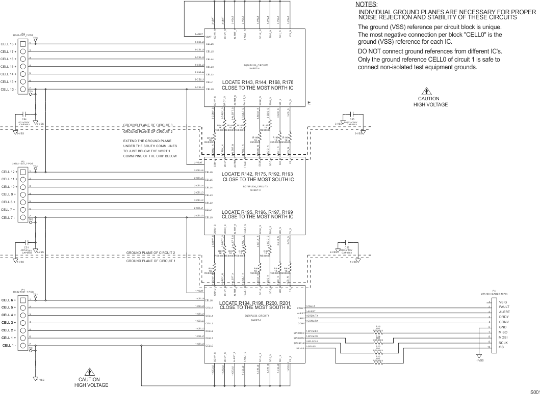 Figure 56. Schematic (Page 1 of 4)
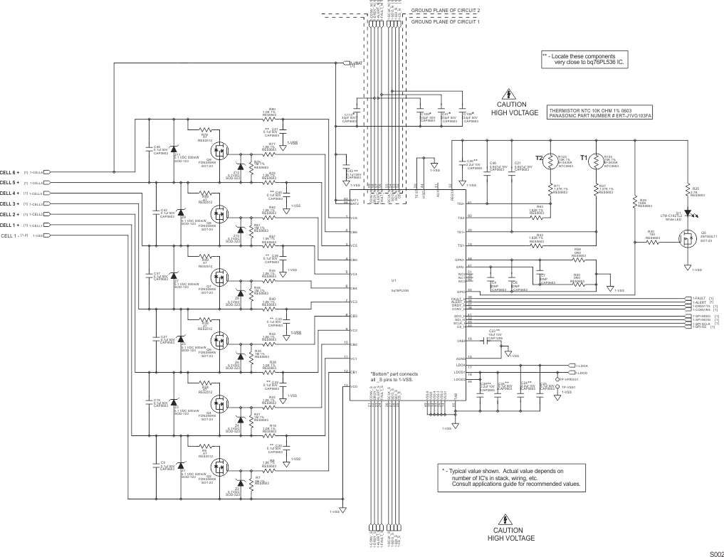 Figure 57. Schematic (Page 2 of 4)
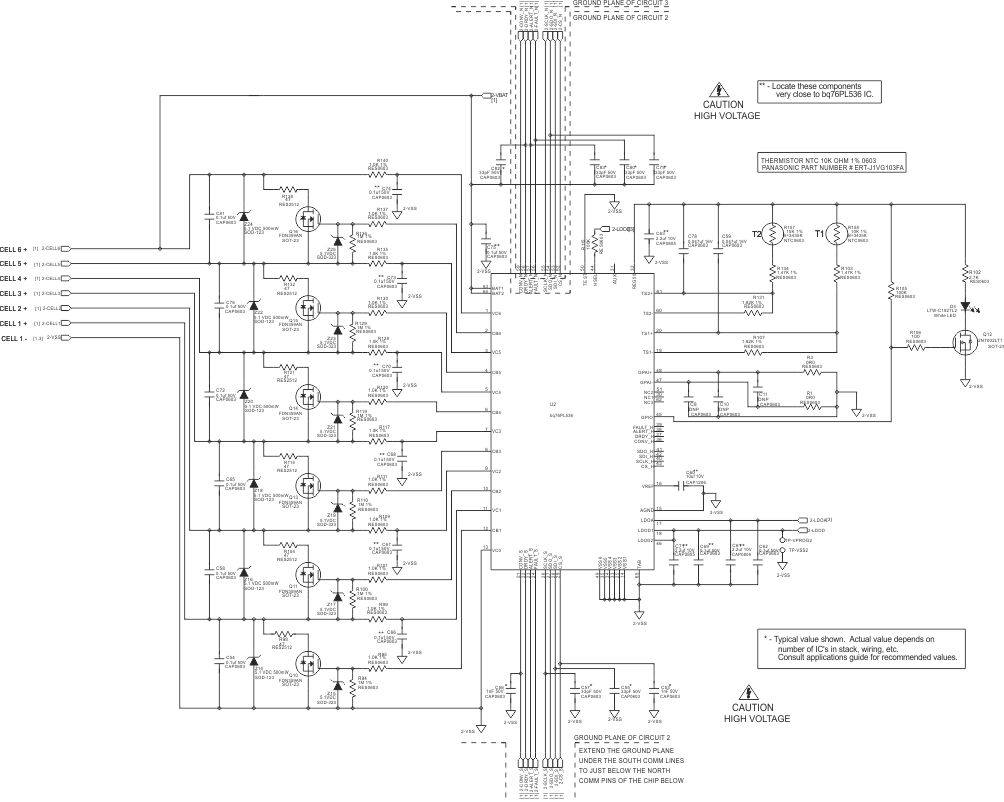 Figure 58. Schematic (Page 3 of 4)
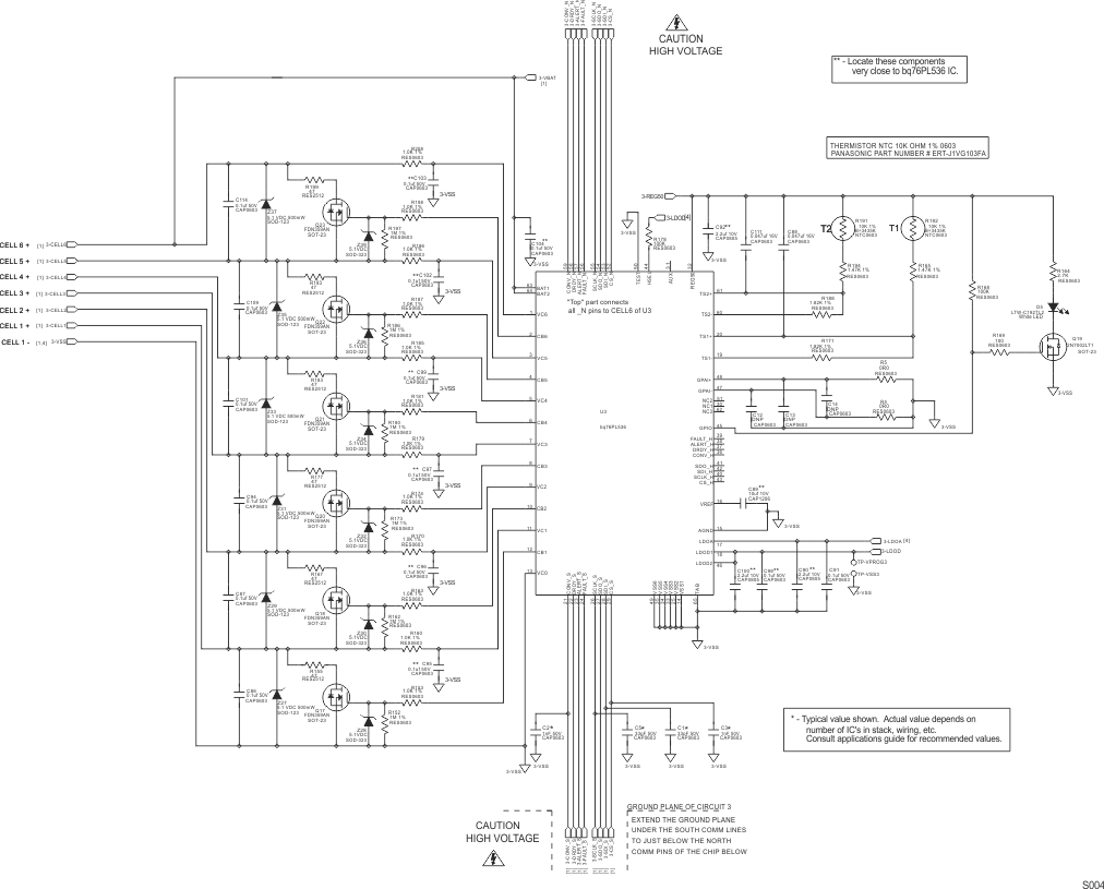 Figure 59. Schematic (Page 4 of 4)
8.2.1 Design Requirements
For this design example, use the parameters listed in Table 9.
Table 9. Design Parameters
| PARAMETER | DESCRIPTION | EXAMPLE VALUE | UNIT |
|---|---|---|---|
| CEMI | EMI Capacitor | 3300 | pF |
| CFILT | Filter Capacitor | 0.1 | µF |
| CIN | Input Capacitor | 0.1 | µF |
| CREGOUT | REGOUT Capacitor | 2.2 (minimum) | µF |
| CVDDA_1 | Internal analog 5-V LDO bypass connection 1 | 2.2 | µF |
| CVDDA_2 | Internal analog 5-V LDO bypass connection 2 | 0.2 | µF |
| CVDD_D_1 | Capacitor for internal digital 5-V LDO bypass connection 1 | 2.2 | µF |
| CVDD_D_2 | Capacitor for internal digital 5-V LDO bypass connection 2 | 0.2 | µF |
| CVREF | VREF Capacitor | 10 | µF |
| LEMI | EMI Ferrite Resistor | 500 | Ω |
| RBAL | Balance Resistor | 47 | Ω |
| RIN | Input Resistor | 1 | kΩ |
| RPULL1-RPULL3 | Pullup Resistors for digital open-drain I/O | 10 | kΩ |
| RPULL4-RPULL5 | Pullup Resistors for general-purpose (differential) analog input (GPAI), connect to VSS if unused | kΩ |
8.2.2 Detailed Design Procedure
Use the following for the procedure for the recommended front-end circuit:
- Select the RC filter closest to the cell for filter requirements. Additional poles can be added with a differential capacitor to get very low fc.
- ADC is calibrated to use RIN = 1 kΩ and CIN = 0.1 µF.
- Select Zener diode for lowest possible reverse leakage.
- A balance FET gate-protection diode is required (available internally).
- Select the capacitors for LDO Filters according to Table 9.
- LDO1 and LDO2 require a 2.2-µF ceramic capacitor for stability. These pins are tied together internally. Tie LDO1 to LDOD2 externally.
- For pullup supply, the following information applies:
- REG50 turns off in SLEEP mode
- Use LDOD for pullups in normal use
- Use REG50 for programming EEPROM (LDOD will see 7 V)
- Connect GPAI+ and GPA– to VSS if unused
- Select low impedance and polarized connectors. Numbered or colored connectors are also good options.
- Select the input Zener TVS so that it clamps below 5.6 Vdc, with low-leakage current, and must be able to handle transient surge energy
- Select capacitors based on temperature and environment with voltages well above the operating voltage
- Select balancing MOSFETs according to the following:
- Low turn on threshold voltage (must turn on with the lowest cell voltage)
- Drain-to-source voltage and gate-to-source voltage
- Power dissipation
- Current based on selected bleed resistor value
- Select the Bleed Resistor according to the following:
- Value based on desired current
- Wattage to handle the current and temperature rise such as 4.2 V × 47 = 0.089 A ∴ 0.37 W)
8.2.3 Application Curves
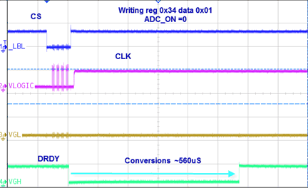
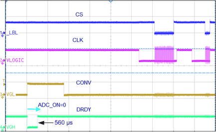
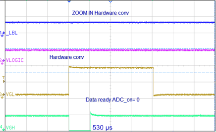
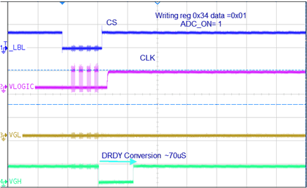
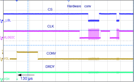
9 Power Supply Recommendations
9.1 Power Supply Decoupling
The LDOA, LDOD1, LDOD2 and REG50 pins all require a 2.2-µF ceramic capacitor to be placed as closely as possible to the respective pins to optimize stability. bq76PL536A-Q1 requires a power supply with between 7.2 V to 27 V inputs. When fewer than six cells are used, see Figure 13 for details.
bq76PL536A-Q1 requires a power supply between 7.2 V to 27 V inputs. When fewer than 6 cells are used, see Figure 13 for details.
10 Layout
10.1 Layout Guidelines
For typical applications, the following guidelines and practices should be followed closely:
- VREF and AGND pins require a high-quality 10-µF capacitor be connected between them, in very close physical proximity to the device pins, using short track lengths to minimize the effects of track inductance on signal quality.
- The AGND pin should be connected to VSS. Device VSS connections should be brought to a single point close to the IC to minimize layout-induced errors. The device tab should also be connected to this point, and is a convenient common VSS location. The internal VREF should not be used externally to the device by user circuits.
- The internal analog supply should be bypassed at the LDOA pin with a good-quality, low-ESR, 2.2-µF ceramic capacitor.
- The bq76PL536A-Q1 has a low-dropout (LDO) regulator provided to power the thermistors and other external circuitry. The input for this regulator is VBAT. The output of REG50 is typically 5 V. A minimum 2.2-µF capacitor is required for stable operation. The output is internally current-limited and is reduced to near zero, if excess current is drawn, causing die temperatures to rise to unacceptable levels. The 2.2-µF output capacitor is required whether REG50 is used in the design or not. REG50 is disabled in SLEEP mode, may be turned off under thermal-shutdown conditions, and therefore should not be used as a pull-up source for terminating device pins where required.
- The bq76PL536A-Q1 includes a general-purpose input/output pin controlled by the IO_CONTROL[GPIO_OUT] bit. The state of this bit is reflected on the pin. To use the pin as an input, program GPIO_OUT to a 1, and then read the IO_CONTROL[GPIO_IN] bit. A pull-up (10 kΩ–1 MΩ, typical) is required on this pin if used as an input. If the pull-up is not included in the design, system firmware must program a 0 in IO_CONTROL[GPIO_OUT] to prevent excess current draw from the floating input. Use of a pull-up is recommended in all designs to prevent an unintentional increase in current draw.
- Device-to-device (D2D) communications makes use of a unique, current-mode interface which provides common-mode voltage isolation between successive bq76PL536A-Q1s. This vertical bus (VBUS) is found on the _N and corresponding _S pins. It provides high-speed I/O for both the SPI bus and the direct I/O pins CONV and DRDY. The current-mode interface minimizes the effects of wiring capacitance on the interface speed. The _S (south-facing) pins connect to the next-lower device (operating at a lower potential) in the stack of bq76PL536A-Q1s. The _N (North facing) pins connect to the next-higher device. The pins cannot be swapped; _S always points South, and _N always point North. The _S and _N pins are interconnected to the pin with the same name, but opposite suffix.
- All pins operate within the voltages present at the BAT and VSS pins.
- The maximum SCLK frequency is limited by the number of devices in the vertical stack and other factors. Each device imposes an approximately 30-ns delay on the round trip communications speed; that is, from SCLK rise time (an input to all devices) to the SDO pin transition time requires approximately 30 ns per device. The designer must add to this the delay caused by the PCB trace (in turn determined by the material and layout), any connectors in series with the connection, and any other wiring or cabling between devices in the system.
- When designing the layout, several considerations need to be taken into account.
- First, in a stacked system, individual ground planes are necessary for proper noise rejection and stability of the circuits.
- Second, the ground (VSS) reference per circuit block is unique. The most negative connection, per block “CELL0”, is the ground (VSS) reference for each IC. Do not connect ground references from different ICs. Only the ground reference CELL0, of the most southerly IC, is safe to connect non-isolated test equipment grounds.
NOTE
Because the LDODx inputs are pulled to approximately 7 V during programming, programming time MUST be < 50 ms.
CAUTION
Be careful as the BAT and VSS pins may be several hundred volts above system ground, depending on their position in the stack.
NOTE
North (_N) pins of the top, most-positive device in the stack, should be connected to the BAT1(2) pins of the device for correct operation of the string. South (_S) pins of the lowest, most-negative device in the stack, should be connected to VSS of the device.
The PowerPAD™ package is a thermally enhanced standard-size IC package designed to eliminate the use of bulky heat sinks and slugs traditionally used in thermal packages. This package can be easily mounted using standard printed circuit board (PCB) assembly techniques, and can be removed and replaced using standard repair procedures. See Figure 65.
The PowerPAD™ package is designed so that the lead frame die pad (or thermal pad) is exposed on the bottom of the IC. This provides an extremely low-thermal resistance (RθJC) path between the die and the exterior of the package. The thermal pad on the bottom of the IC can then be soldered directly to the printed circuit board (PCB), using the PCB as a heat sink. In addition, through the use of thermal bias, the thermal pad can be directly connected to a ground plane or special heat sink structure designed into the PCB.
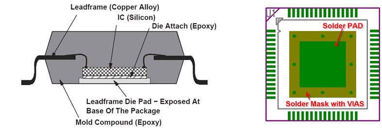 Figure 65. Section View of PowerPAD™ Package and Top View of Solder Mask and Pad
10.2 Layout Example
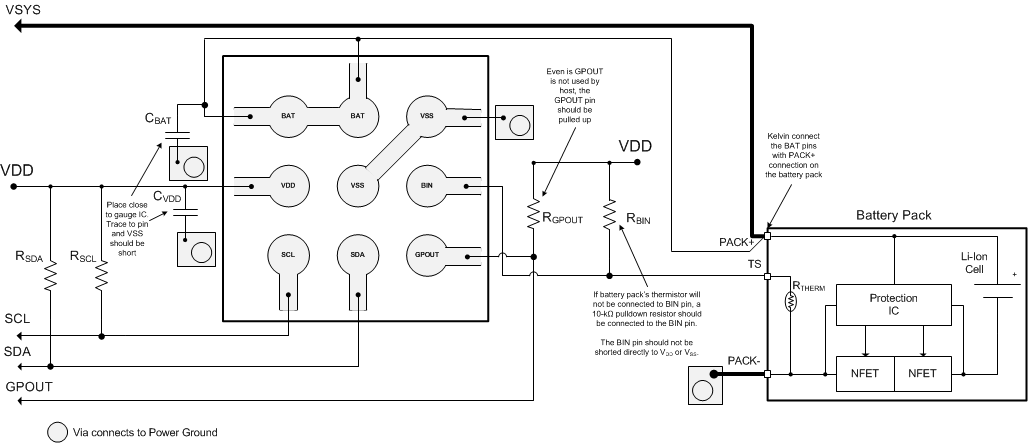 Figure 66. Layout
