-
PCM514x2 VRMS DirectPath™、112/106dB 音频立体声 DAC, 具有 32 位、384kHz 脉冲编码调制 (PCM) 接口
- 1 特性
- 2 应用
- 3 说明
- 4 修订历史记录
- 5 Device Comparison
- 6 Pin Configuration and Functions
-
7 Specifications
- 7.1 Absolute Maximum Ratings
- 7.2 ESD Ratings
- 7.3 Recommended Operating Conditions
- 7.4 Thermal Information
- 7.5 Electrical Characteristics
- 7.6 Timing Requirements: SCK Input
- 7.7 Timing Requirements: PCM Audio Data
- 7.8 Timing Requirements: I2S Master
- 7.9 Timing Requirements: XSMT
- 7.10 Switching Characteristics
- 7.11 Typical Characteristics
-
8 Detailed Description
- 8.1 Overview
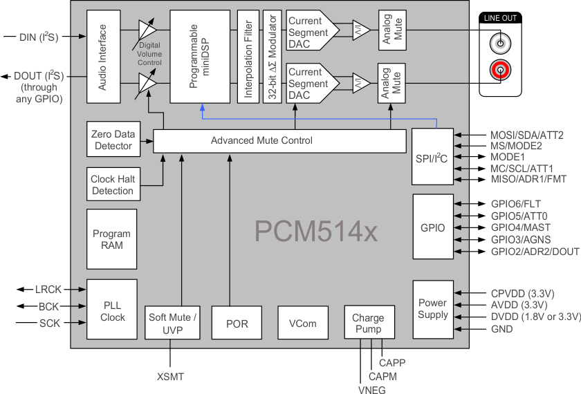
- 8.2 Functional Block Diagram
- 8.3
Feature Description
- 8.3.1 Terminology
- 8.3.2 Audio Data Interface
- 8.3.3 XSMT Pin (Soft Mute / Soft Un-Mute)
- 8.3.4 Audio Processing
- 8.3.5 DAC Outputs
- 8.3.6
Reset and System Clock Functions
- 8.3.6.1 Clocking Overview
- 8.3.6.2 Clock Slave Mode With Master and System Clock (SCK) Input (4 Wire I2S)
- 8.3.6.3 Clock Slave Mode With BCK PLL to Generate Internal Clocks (3-Wire PCM)
- 8.3.6.4 Clock Generation Using the PLL
- 8.3.6.5 PLL Calculation
- 8.3.6.6 Clock Master Mode from Audio Rate Master Clock
- 8.3.6.7 Clock Master from a Non-Audio Rate Master Clock
- 8.4 Device Functional Modes
- 8.5 Programming
- 9 Application and Implementation
- 10Power Supply Recommendations
- 11Layout
- 12Register Maps
- 13器件和文档支持
- 14机械、封装和可订购信息
- 重要声明
PCM514x2 VRMS DirectPath™、112/106dB 音频立体声 DAC, 具有 32 位、384kHz 脉冲编码调制 (PCM) 接口
1 特性
- 可编程 miniDSP
- 市场领先的低带外噪声特性
- 可选数字滤波器延迟与性能
- 无需隔离直流电流的电容器
- 集成的负电荷泵
- 智能静音系统;软斜升或斜降搭配模拟静音,实现 120dB 静音信噪比 (SNR)
- 具有 BCK 基准的集成高性能音频锁相环 (PLL),可在内部生成 SCK
- 接受 16 位、20 位、24 位和 32 位音频数据
- 脉冲编码调制 (PCM) 数据格式:I2S、左对齐、右对齐、时分复用 (TDM)/数字信号处理 (DSP)
- 通用串行接口 (SPI) 或者 I2C 控制
- 软件或者硬件配置
- 当 LRCK 和 BCK 被置为无效时,自动进入省电模式
- 1.8V 或 3.3V 故障安全低电压互补金属氧化物半导体 (LVCMOS) 数字输入
- 单电源供电运行:
3.3V(模拟),1.8V 或 3.3V(数字) - 集成型加电复位
- 小型28-pin TSSOP封装
2 应用
- A/V 接收器
- DVD,BD 播放器
- HDTV 接收器
- 需要 2 VRMS 音频输出的应用
3 说明
PCM514x 器件属于单片 CMOS 集成电路系列,由立体声数模转换器 (DAC) 和采用薄型小外形尺寸 (TSSOP) 封装的附加支持电路组成。PCM514x 使用 TI 最新一代高级分段 DAC 架构产品,可实现出色的动态性能并提升针对时钟抖动的耐受度。
PCM514x 系列器件集成了一个完全可编程的 miniDSP 内核,允许开发人员将滤波器、动态范围控件、定制插值器等各类 功能 集成到相关产品中。
PCM514x 提供 2.1 VRMS 中央接地输出(设计人员无需在输出上连接隔直电容)以及传统意义上与单电源线路驱动器相关的外部静音电路。
集成的线路驱动器支持低至 1kΩ 的负载,允许 PCM514x 驱动多达 10 个并联产品(例如 LCD TV、DVDR 和 AV 接收器),性能优于所有其他基于电荷泵的线路驱动器。
器件上集成的 PLL 免除了对于系统时钟(通常称为主时钟)的需要,从而实现一个 3 线制 I2C 连接并减少了系统电磁干扰 (EMI)。
器件信息
| 器件名称 | 封装 | 封装尺寸(标称值) |
|---|---|---|
| PCM5141 | TSSOP (28) | 9.70mm x 4.40mm |
| PCM5142 |
.
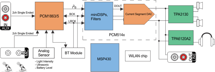
简化系统图
4 修订历史记录
Changes from A Revision (September 2012) to B Revision
- Deleted 无喀嗒和噼啪声的内部控制,用于更改采样率或暂停时钟,... 无喀嗒和噼啪声操作Go
- Changed “接受 16 位、24 位和 32 位音频数据”至“接受 16 位、20 位、24 位和 32 位音频数据”Go
- Added 引脚配置和功能部分,ESD 额定值表,特性 说明部分,器件功能模式,应用和实施部分,电源相关建议部分,布局部分,器件和文档支持部分以及机械、封装和可订购信息部分Go
- Clarified Pin Functions table.Go
- Changed Operating temperature to Operating junction temperature in Absolute Maximum RatingsGo
- Deleted redundant PLL specification in Recommended Operating Conditions Go
- Deleted Intelligent clock error... and ...for pop-free performance in the Overview section.Go
- Added note on instruction cycles to PCM512x Audio Processing.Go
- Deleted text The Graphical Development Environment consists of number of Hybrid Flows that can be downloaded to the device and run on the miniDSP. From: Software Go
- Added note on instruction cycles in Fixed Audio Processing Flow (Program 5).Go
- Changed Ouptut to OutputGo
- Deleted VREF mode provides 2.1Vrms full-scale output at both AVDD levels.Go
- Clarified clock generation explanation in Reset and System Clock FunctionsGo
- Clarified external SCK discussion in Clock Slave Mode with BCK PLL to Generate Internal Clocks (3-Wire PCM).Go
- Deleted The PCM514x disables the internal PLL when an external SCK is supplied.Go
5 Device Comparison
Table 1. Differences Between PCM514x Devices
| PART NUMBER | DYNAMIC RANGE | SNR | THD |
|---|---|---|---|
| PCM5142A | 112 dB | 112 dB | –93 dB |
| PCM5141A | 106 dB | 106 dB | –92 dB |
Table 2. Typical Performance (3.3-V Power Supply)
| PARAMETER | PCM5142 / PCM5141 |
|---|---|
| SNR | 112 / 106 dB |
| Dynamic range | 112 /106 dB |
| THD+N at –1 dBFS | –93/ –92 dB |
| Full-scale single-ended output | 2.1 VRMS (GND center) |
| Normal 8× oversampling digital filter latency | 20tS |
| Low latency 8× oversampling digital filter latency | 3.5tS |
| Sampling frequency | 8 kHz to 384 kHz |
| System clock multiples (fSCK): 64, 128, 192, 256, 384, 512, 768, 1024, 1152, 1536, 2048, 3072 | Up to 50 MHz |
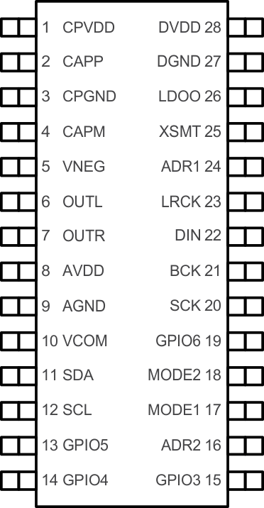
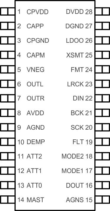
6 Pin Configuration and Functions
RHB Package
I2C Mode
(MODE1 tied to DGND and MODE2 tied to DVDD)
Top View
RHB Package
Hardwired Mode
(MODE1 tied to DGND, MODE2 tied to DGND)
Top View
RHB Package
SPI Mode
(MODE1 tied to DVDD)
Top View
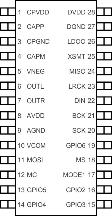
Table 3. Gain and Attenuation in Hardwired Mode
| ATT PIN CONDITION (ATT2 : ATT1 : ATT0) | GAIN AND ATTENUATION LEVEL |
|---|---|
| ( 0 0 0 ) | 0 dB |
| ( 0 0 1 ) | 3 dB |
| ( 0 1 0 ) | 6 dB |
| ( 0 1 1 ) | 9 dB |
| ( 1 0 0 ) | 12 dB |
| ( 1 0 1 ) | 15 dB |
| ( 1 1 0 ) | –6 dB |
| ( 1 1 1 ) | –3 dB |
6.1 Pin Functions
| PIN | I/O | DESCRIPTION | |||||
|---|---|---|---|---|---|---|---|
| NAME | MODE, NO. | ||||||
| I2C | SPI | HW | |||||
| CPVDD | 1 | 1 | 1 | - | Charge pump power supply, 3.3 V | ||
| CAPP | 2 | 2 | 2 | O | Charge pump flying capacitor terminal for positive rail | ||
| CPGND | 3 | 3 | 3 | - | Charge pump ground | ||
| CAPM | 4 | 4 | 4 | O | Charge pump flying capacitor terminal for negative rail | ||
| VNEG | 5 | 5 | 5 | O | Negative charge pump rail terminal for decoupling, –3.3 V | ||
| OUTL | 6 | 6 | 6 | O | Analog output from DAC left channel | ||
| OUTR | 7 | 7 | 7 | O | Analog output from DAC right channel | ||
| AVDD | 8 | 8 | 8 | - | Analog power supply, 3.3 V | ||
| AGND | 9 | 9 | 9 | - | Analog ground | ||
| VCOM | 10 | 10 | – | O | I2C, SPI | VCOM output (optional mode selected by register; default setting is VREF mode.) When in VREF mode (default), this pin ties to GND. When in VCOM mode, decoupling capacitor to GND is required. | |
| DEMP | – | – | 10 | I | HW | DEMP: De-emphasis control for 44.1-kHz sampling rate: Off (Low) / On (High) | |
| SDA | 11 | – | – | I/O | I2C | Data for I2C(1)(2) | |
| MOSI | – | 11 | – | I | SPI | Input data for SPI(2) | |
| ATT2 | – | – | 11 | HW | Digital gain and attenuation control pin | ||
| SCL | 12 | – | – | I | I2C | Input clock for I2C(2) | |
| MC | – | 12 | – | SPI | Input clock for SPI(2) | ||
| ATT1 | – | – | 12 | HW | Digital gain and attenuation control pin | ||
| GPIO5 | 13 | 13 | – | I/O | I2C, SPI | General purpose digital input and output port (3) | |
| ATT0 | – | – | 13 | HW | Digital gain and attenuation control pin | ||
| GPIO4 | 14 | 14 | – | I/O | I2C, SPI | General purpose digital input and output port (3) | |
| MAST | – | – | 14 | HW | I2S Master clock select pin : Master (High) BCK/LRCK outputs, Slave (Low) BCK/LRCK inputs | ||
| GPIO3 | 15 | 15 | – | I/O | I2C, SPI | General purpose digital input and output port (3) | |
| AGNS | – | – | 15 | HW | Analog gain selector : 0-dB 2-VRMS output (Low), –6-dB 1-VRMS output (High) | ||
| ADR2 | 16 | – | – | I/O | I2C | 2nd LSB address select bit for I2C | |
| GPIO2 | – | 16 | – | SPI | General purpose digital input and output port | ||
| DOUT | – | – | 16 | O | HW | General Purpose Output (Low level) | |
| MODE1 | 17 | 17 | 17 | I | Mode control selection pin (2)
MODE1 = Low, MODE2 = Low : Hardwired mode MODE1 = Low, MODE2 = High: I2C mode MODE1 = High: SPI mode |
||
| MODE2 | 18 | – | 18 | I2C, HW | MODE2 | ||
| MS | – | 18 | – | I | SPI | MS pin (chip select for SPI) | |
| GPIO6 | 19 | 19 | – | I/O | I2C, SPI | General purpose digital input and output port | |
| FLT | – | – | 19 | I | HW | Filter select : Normal latency (Low) / Low latency (High) | |
| SCK | 20 | 20 | 20 | I | System clock input(2) | ||
| BCK | 21 | 21 | 21 | I/O | Audio data bit clock input (slave) or output (master)(2) | ||
| DIN | 22 | 22 | 22 | I | Audio data input(2) | ||
| LRCK | 23 | 23 | 23 | I/O | Audio data word clock input (slave) or output (master)(2) | ||
| ADR1 | 24 | – | – | I/O | I2C | LSB address select bit for I2C | |
| MISO (GPIO1) | – | 24 | – | SPI | Primary output data for SPI readback. Secondary; general purpose digital input/output port controlled by register | ||
| FMT | – | – | 24 | HW | Audio format selection : I2S (Low) / Left justified (High) | ||
| XSMT | 25 | 25 | 25 | I | Soft mute control Soft mute(2) (Low) / soft un-mute (High) | ||
| LDOO | 26 | 26 | 26 | - | Internal logic supply rail terminal for decoupling, 1.8 V | ||
| DGND | 27 | 27 | 27 | - | Digital ground | ||
| DVDD | 28 | 28 | 28 | - | Digital power supply, 3.3 V or 1.8 V | ||
7 Specifications
7.1 Absolute Maximum Ratings
over operating free-air temperature range (unless otherwise noted)| MIN | MAX | UNIT | ||
|---|---|---|---|---|
| Supply voltage | AVDD, CPVDD, DVDD | –0.3 | 3.9 | V |
| LDO with DVDD at 1.8 V | –0.3 | 2.25 | ||
| Digital input voltage | DVDD at 1.8 V | –0.3 | 2.25 | V |
| DVDD at 3.3 V | –0.3 | 3.9 | ||
| Analog input voltage | –0.3 | 3.9 | V | |
| Operating junction temperature, TJ | –40 | 130 | °C | |
| Storage temperature, Tstg | –65 | 150 | °C | |
7.2 ESD Ratings
| VALUE | UNIT | |||
|---|---|---|---|---|
| V(ESD) | Electrostatic discharge | Human-body model (HBM), per ANSI/ESDA/JEDEC JS-001(1) | ±2000 | V |
| Charged-device model (CDM), per JEDEC specification JESD22-C101(2) | ±750 | |||
7.3 Recommended Operating Conditions
| MIN | NOM | MAX | UNIT | ||||
|---|---|---|---|---|---|---|---|
| AVDD | Analog power supply voltage | Referenced to AGND(1) | VCOM mode | 3 | 3.3 | 3.46 | V |
| VREF mode | 3.2 | 3.3 | 3.46 | ||||
| DVDD | Digital power supply voltage | Referenced to DGND(1) | 1.8 V DVDD | 1.65 | 1.8 | 1.95 | V |
| 3.3 V DVDD | 3.1 | 3.3 | 3.46 | ||||
| CPVDD | Charge pump supply voltage | Referenced to CPGND(1) | 3.1 | 3.3 | 3.46 | V | |
| MCLK | Master clock frequency | 50 | MHz | ||||
| LOL, LOR | Stereo line output load resistance | 1 | 10 | kΩ | |||
| CLOUT | Digital output load capacitance | 10 | pF | ||||
| TJ | Operating junction temperature | –40 | 130 | °C | |||
7.4 Thermal Information
| THERMAL METRIC(1) | PCM512x | UNIT | ||
|---|---|---|---|---|
| RHB (TSSOP) | ||||
| 32 PINS | ||||
| RθJA | Junction-to-ambient thermal resistance | 72.2 | °C/W | |
| RθJC(top) | Junction-to-case(top) thermal resistance | 17.5 | °C/W | |
| RθJB | Junction-to-board thermal resistance | 35.0 | °C/W | |
| ψJT | Junction-to-top characterization parameter | 0.4 | °C/W | |
| ψJB | Junction-to-board characterization parameter | 34.5 | °C/W | |
7.5 Electrical Characteristics
TA = 25°C, AVDD = CPVDD = DVDD = 3.3 V, fS = 48 kHz, system clock = 512 fS and 24-bit data (unless otherwise noted).| PARAMETER | TEST CONDITIONS | MIN | TYP | MAX | UNIT | |
|---|---|---|---|---|---|---|
| Resolution | 16 | 24 | 32 | Bits | ||
| DIGITAL INPUT/OUTPUT | ||||||
| Logic Family: 3.3-V LVCMOS Compatible | ||||||
| VIH | Input logic level, high | 0.7 × DVDD | V | |||
| VIL | Input logic level, low | 0.3 × DVDD | V | |||
| IIH | Input logic current, high | VIN = VDD | 10 | µA | ||
| IIL | Input logic current, low | VIN = 0 V | –10 | µA | ||
| VOH | Output logic level, high | IOH = –4 mA | 0.8 × DVDD | V | ||
| VOL | Output logic level, low | IOL = 4 mA | 0.22 × DVDD | V | ||
| Logic Family 1.8-V LVCMOS Compatible | ||||||
| VIH | Input logic level, high | 0.7 × DVDD | V | |||
| VIL | Input logic level, low | 0.3 × DVDD | V | |||
| IIH | Input logic current, high | VIN = VDD | 10 | µA | ||
| IIL | Input logic current, low | VIN = 0 V | –10 | µA | ||
| VOH | Output logic level, high | IOH = –2 mA | 0.8 × DVDD | V | ||
| VOL | Output logic level, low | IOL = 2 mA | 0.22 × DVDD | V | ||
| DYNAMIC PERFORMANCE (PCM MODE)(1)(2) | ||||||
| THD+N at –1 dB(2) | fS = 48 kHz | –93 | –83 | dB | ||
| fS = 96 kHz | –93 | |||||
| fS = 192 kHz | –93 | |||||
| Dynamic range(2) | EIAJ, A-weighted, fS = 48 kHz | 108 | 112 | dB | ||
| EIAJ, A-weighted, fS = 96 kHz | 112 | |||||
| EIAJ, A-weighted, fS = 192 kHz | 112 | |||||
| Signal-to-noise ratio(2) | EIAJ, A-weighted, fS = 48 kHz | 112 | dB | |||
| EIAJ, A-weighted, fS = 96 kHz | 112 | |||||
| EIAJ, A-weighted, fS = 192 kHz | 112 | |||||
| Signal-to-noise ratio with analog mute(2)(3) | EIAJ, A-weighted, fS = 48 kHz | 113 | 123 | dB | ||
| EIAJ, A-weighted, fS = 96 kHz | 113 | 123 | ||||
| EIAJ, A-weighted, fS = 192 kHz | 113 | 123 | ||||
| Channel separation | fS = 48 kHz | 100 / 95 | 109 / 103 | dB | ||
| fS = 96 kHz | 100 / 95 | 109 / 103 | ||||
| fS = 192 kHz | 100 / 95 | 109 / 103 | ||||
| ANALOG OUTPUT | ||||||
| Single-ended output voltage | 2.1 | VRMS | ||||
| Gain error | –6 | ±2.0 | 6 | % of FSR | ||
| Gain mismatch, channel-to-channel | –6 | ±0.5 | 6 | % of FSR | ||
| Load impedance | 5 | kΩ | ||||
| FILTER CHARACTERISTICS–1: NORMAL (8x) | ||||||
| Pass band | 0.45 × fS | kHz | ||||
| Stop band | 0.55 × fS | kHz | ||||
| Stop band attenuation | –60 | dB | ||||
| Pass-band ripple | ±0.02 | dB | ||||
| Delay time | 20 × tS | s | ||||
| FILTER CHARACTERISTICS–2: LOW LATENCY (8x) | ||||||
| Pass band | 0.47 × fS | kHz | ||||
| Stop band | 0.55 × fS | kHz | ||||
| Stop band attenuation | –52 | dB | ||||
| Pass-band ripple | ±0.0001 | dB | ||||
| Delay time | 3.5 × tS | s | ||||
| FILTER CHARACTERISTICS–3: ASYMMETRIC FIR (8x) | ||||||
| Pass band | 0.4 × fS | kHz | ||||
| Stop band | 0.72 × fS | kHz | ||||
| Stop band attenuation | –52 | dB | ||||
| Pass-band ripple | ±0.05 | dB | ||||
| Delay time | 1.2 × tS | s | ||||
| FILTER CHARACTERISTICS–4: HIGH-ATTENUATION (8x) | ||||||
| Pass band | 0.45 × fS | kHz | ||||
| Stop band | 0.45 × fS | kHz | ||||
| Stop band attenuation | –100 | dB | ||||
| Pass-band ripple | ±0.0005 | dB | ||||
| Delay time | 33.7 × tS | s | ||||
| POWER SUPPLY REQUIREMENTS | ||||||
| DVDD | Digital supply voltage | Target DVDD = 1.8 V | 1.65 | 1.8 | 1.95 | VDC |
| DVDD | Digital supply voltage | Target DVDD = 3.3 V | 3 | 3.3 | 3.6 | VDC |
| AVDD | Analog supply voltage | 3 | 3.3 | 3.6 | VDC | |
| CPVDD | Charge-pump supply voltage | 3 | 3.3 | 3.6 | VDC | |
| IDD | DVDD supply current at 1.8 V | fS = 48 kHz, input is bipolar zero data | 11 | 14 | mA | |
| fS = 96 kHz, input is bipolar zero data | 12 | |||||
| fS = 192 kHz, input is bipolar zero data | 14 | |||||
| IDD | DVDD supply current at 1.8 V | fS = 48 kHz, input is 1 kHz – 1 dBFS data | 11 | 14 | mA | |
| fS = 96 kHz, input is 1 kHz – 1 dBFS data | 12 | |||||
| fS = 192 kHz, input is 1 kHz – 1 dBFS data | 14 | |||||
| IDD | DVDD supply current at 1.8 V(4) | fS = N/A, power-down mode | 0.3 | 0.6 | mA | |
| IDD | DVDD supply current at 3.3 V | fS = 48 kHz, input is bipolar zero data | 12 | 15 | mA | |
| fS = 96 kHz, input is bipolar zero data | 13 | |||||
| fS = 192 kHz, input is bipolar zero data | 15 | |||||
| IDD | DVDD supply current at 3.3 V | fS = 48 kHz, input is 1 kHz – 1 dBFS data | 12 | 15 | mA | |
| fS = 96 kHz, input is 1 kHz – 1 dBFS data | 13 | |||||
| fS = 192 kHz, input is 1 kHz – 1 dBFS data | 15 | |||||
| IDD | DVDD supply current at 3.3 V(4) | fS = N/A, power-down mode | 0.5 | 0.8 | mA | |
| ICC | AVDD + CPVDD supply current | fS = 48 kHz, input is bipolar zero data | 11 | 16 | mA | |
| fS = 96 kHz, input is bipolar zero data | 11 | |||||
| fS = 192 kHz, input is bipolar zero data | 11 | |||||
| ICC | AVDD + CPVDD supply current | fS = 48 kHz, input is 1 kHz – 1 dBFS data | 24 | 32 | mA | |
| fS = 96 kHz, input is 1 kHz – 1 dBFS data | 24 | |||||
| fS = 192 kHz, input is 1 kHz – 1 dBFS data | 24 | |||||
| ICC | AVDD + CPVDD supply current(4) | fS = N/A, power-down mode | 0.2 | 0.4 | mA | |
| Power dissipation, DVDD = 1.8 V | fS = 48 kHz, input is bipolar zero data | 59.4 | 78 | mW | ||
| fS = 96 kHz, input is bipolar zero data | 61.2 | |||||
| fS = 192 kHz, input is bipolar zero data | 64.8 | |||||
| Power dissipation, DVDD = 1.8 V | fS = 48 kHz, input is 1 kHz – 1 dBFS data | 99 | 130.8 | mW | ||
| fS = 96 kHz, input is 1 kHz – 1 dBFS data | 100.8 | |||||
| fS = 192 kHz, input is 1 kHz – 1 dBFS data | 104.4 | |||||
| Power dissipation, DVDD = 1.8 V(4) | fS = N/A, power-down mode | 1.2 | mW | |||
| Power dissipation, DVDD = 3.3 V | fS = 48 kHz, input is bipolar zero data | 79.2 | 103 | mW | ||
| fS = 96 kHz, input is bipolar zero data | 82.5 | |||||
| fS = 192 kHz, input is bipolar zero data | 89.1 | |||||
| Power dissipation, DVDD = 3.3 V | fS = 48 kHz, input is 1 kHz – 1 dBFS data | 118.8 | 155 | mW | ||
| fS = 96 kHz, input is 1 kHz – 1 dBFS data | 122.1 | |||||
| fS = 192 kHz, input is 1 kHz – 1 dBFS data | 128.7 | |||||
| Power dissipation, DVDD = 3.3 V(4) | fS = N/A, power-down mode | 2.3 | 4 | mW | ||
7.6 Timing Requirements: SCK Input
Figure 1 shows the timing requirements for the system clock input. For optimal performance, use a clock source with low phase jitter and noise.| MIN | NOM | MAX | UNIT | |||
|---|---|---|---|---|---|---|
| tSCY | System clock pulse cycle time | 20 | 1000 | ns | ||
| tSCKH | System clock pulse width, high | DVDD = 1.8 V | 8 | ns | ||
| DVDD = 3.3 V | 9 | |||||
| tSCKL | System clock pulse width, low | DVDD = 1.8 V | 8 | ns | ||
| DVDD = 3.3 V | 9 | |||||
7.7 Timing Requirements: PCM Audio Data
| MIN | NOM | MAX | UNIT | ||
|---|---|---|---|---|---|
| tBCY | BCK Pulse Cycle Time | 40 | ns | ||
| tBCL | BCK Pulse Width LOW | 16 | ns | ||
| tBCH | BCK Pulse Width HIGH | 16 | ns | ||
| tBL | BCK Rising Edge to LRCK Edge | 8 | ns | ||
| tBCK | BCK frequency | 24.576 | MHz | ||
| tLB | LRCK Edge to BCK Rising Edge | 8 | ns | ||
| tDS | DATA Set Up Time | 8 | ns | ||
| tDH | DATA Hold Time | 8 | ns | ||
| tDOD | DATA delay time from BCK falling edge | 15 | ns | ||
7.8 Timing Requirements: I2S Master
| MIN | NOM | MAX | UNIT | ||
|---|---|---|---|---|---|
| tBCY | BCK Pulse Cycle Time | 40 | ns | ||
| tBCL | BCK Pulse Width LOW | 16 | ns | ||
| tBCH | BCK Pulse Width HIGH | 16 | ns | ||
| tBCK | BCK frequency at DVDD = 3.3 V | 24.576 | MHz | ||
| tBCK(1.8V) | BCK frequency at DVDD = 1.8 V | 12.288 | MHz | ||
| tLRD | LRCKx delay time from BCKx falling edge | –10 | 20 | ns | |
| tDS | DATA Set Up Time | 8 | ns | ||
| tDH | DATA Hold Time | 8 | ns | ||
| tDOD | DATA delay time from BCK falling edge at DVDD = 3.3 V | 15 | ns | ||
| tDOD(1.8V) | DATA delay time from BCK falling edge at DVDD = 1.8 V | 20 | ns | ||
7.9 Timing Requirements: XSMT
| MIN | NOM | MAX | UNIT | ||
|---|---|---|---|---|---|
| tr | Rise time | 20 | ns | ||
| tf | Fall time | 20 | ns | ||
7.10 Switching Characteristics
over operating free-air temperature range (unless otherwise noted)| PARAMETER | TEST CONDITIONS | MIN | TYP | MAX | UNIT | |
|---|---|---|---|---|---|---|
| DATA FORMAT (PCM MODE) | ||||||
| Audio data interface format | I2S, left-justified, right-justified, and TDM | |||||
| Audio data bit length | 16, 20, 24, 32-bit acceptable | |||||
| Audio data format | MSB first, twos-complement | |||||
| fS | Sampling frequency(1) | 8 | 384 | kHz | ||
| CLOCKS | ||||||
| System clock frequency | 64, 128, 192, 256, 384, 512, 768, 1024, 1152, 1536, 2048, or 3072 fSCK, up to 50 Mhz |
|||||
| PLL input frequency (2) | Clock divider uses fractional divide D > 0, P=1 |
6.7 | 20 | MHz | ||
| Clock divider uses integer divide D = 0, P=1 |
1 | 20 | MHz | |||
 Figure 1. Timing Requirements for SCK Input
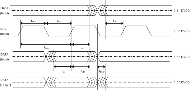 Figure 2. PCM514x Serial Audio Timing - Slave
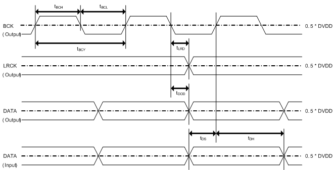 Figure 3. PCM514x Serial Audio Timing - I2S Master
 Figure 4. XSMT Timing for Soft Mute and Soft Un-Mute
7.11 Typical Characteristics
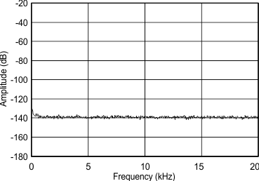
Consumer grade (non-Q1) devices are specified for TA = 25°C, AVDD = CPVDD = DVDD = 3.3 V, fS = 48 kHz, system clock = 512 fS and 24-bit data (unless otherwise noted).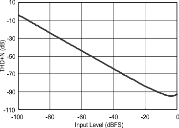
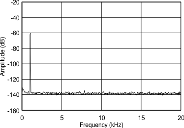
(–60 dBFS) from DC to 20 kHz
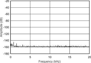
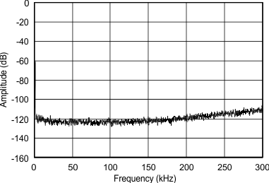
(–60 dBFS) from DC to 300 kHz
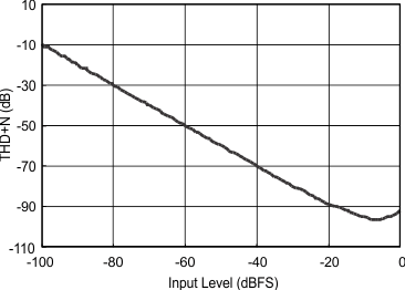
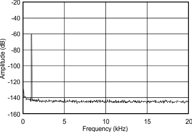
(–60 dBFS) from DC to 20 kHz
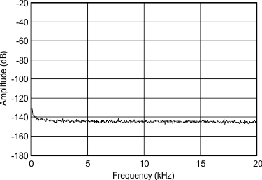
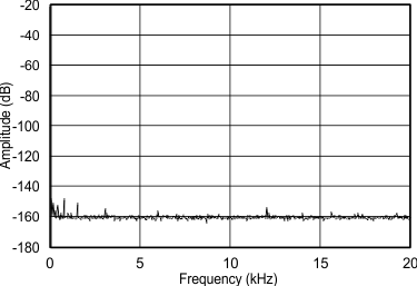
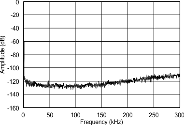
(–60 dBFS) from DC to 300 kHz
8 Detailed Description
8.1 Overview
The integrated PLL on the device provided adds the flexibility to remove the system clock (commonly known as master clock), allowing a 3-wire I2S connection and reducing system EMI. In addition, the PLL is completely programmable, allowing the device to become the I2S clock master and drive a DSP serial port as a slave. The PLL also accepts a non-standard clock (up to 50 MHz) as a source to generate the audio related clock (for example, 24.576 MHz).
Powersense undervoltage protection utilizes a two-level mute system. Upon clock error or system power failure, the device digitally attenuates the data (or last known good data) and then mutes the analog circuit.
Compared with existing DAC technology, the PCM514x devices offer up to 20-dB lower out-of-band noise, reducing EMI and aliasing in downstream amplifiers/ADCs (from traditional 100-kHz OBN measurements to
3 MHz).
The PCM514x devices accept industry-standard audio data formats with 16- to 32-bit data. Sample rates up to 384 kHz are supported.
8.2 Functional Block Diagram
8.3 Feature Description
8.3.1 Terminology
Control registers in this data sheet are given by REGISTER BIT/BYTE NAME (Page.x HEX ADDRESS). SE refers to single-ended analog inputs. SCK (System Clock) and MCLK (Master Clock) are used interchangeably. Sampling frequency is symbolized by fS. Full scale is symbolized by FS. Sample time as a unit is symbolized by tS.
8.3.2 Audio Data Interface
8.3.2.1 Audio Serial Interface
The audio interface port is a 3-wire serial port with the signals LRCK, BCK, and DIN. BCK is the serial audio bit clock, used to clock the serial data present on DIN into the serial shift register of the audio interface. Serial data is clocked into the PCM514x on the rising edge of BCK. LRCK is the serial audio left/right word clock. LRCK polarity for left/right is given by the format selected.
Table 4. PCM514x Audio Data Formats, Bit Depths and Clock Rates
| CONTROL MODE | FORMAT | DATA BITS | MAX LRCK FREQUENCY [fS] | SCK RATE [x fS] | BCK RATE [x fS] |
|---|---|---|---|---|---|
| Software Control (SPI or I2S) |
I2S/LJ | 32, 24, 20, 16 | Up to 192 kHz | 128 – 3072 | 64, 48, 32 |
| 384 kHz | 64, 128 | 64, 48, 32 | |||
| TDM/DSP | 32, 24, 20, 16 | Up to 48 kHz | 128 – 3072 | 128, 256 | |
| 96 kHz | 128 – 512 | 128, 256 | |||
| 192 kHz | 128, 192, 256 | 128 | |||
| Hardware Control | I2S/LJ | 32, 24, 20, 16 | Up to 192 kHz | 128 – 3072 | 64, 48, 32 |
| 384 kHz | 64, 128 | 64, 48, 32 |
The PCM514x requires the synchronization of LRCK and system clock, but does not need a specific phase relation between LRCK and system clock.
If the relationship between LRCK and system clock changes more than ±5 SCK, internal operation (using an onchip oscillator) is initialized within one sample period and analog outputs are forced to the bipolar zero level until resynchronization between LRCK and system clock is completed.
If the relationship between LRCK and BCK are invalid more than 4 LRCK periods, internal operation (using an onchip oscillator) is initialized within one sample period and analog outputs are forced to the bipolar zero level until resynchronization between LRCK and BCK is completed.
8.3.2.2 PCM Audio Data Formats
The PCM514x supports industry-standard audio data formats, including standard I2S and left-justified. Data formats are selected via Register (Pg0Reg40). All formats require binary twos-complement, MSB-first audio data; up to 32-bit audio data is accepted.
The PCM514x also supports right-justified and TDM/DSP in software control mode. I2S, LJ, RJ, and TDM/DSP are selected using Register (Pg0Reg40). All formats require binary twos-complement, MSB-first audio data. Up to 32 bits are accepted. Default setting is I2S and 24-bit word length.
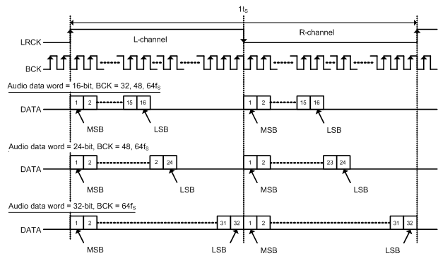 Figure 15. Left-Justified Audio Data Format
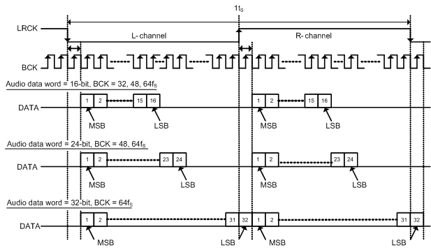
The following data formats are only available in software mode.
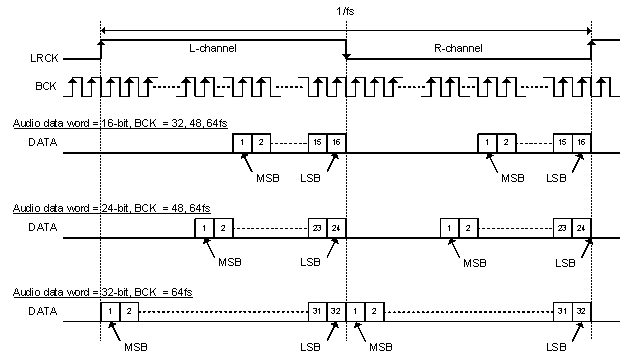
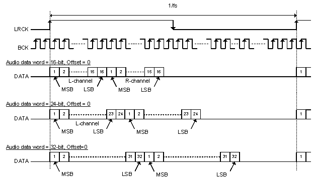
NOTE
In TDM Modes, Duty Cycle of LRCK should be 1x BCK at minimum. Rising edge is considered frame start.
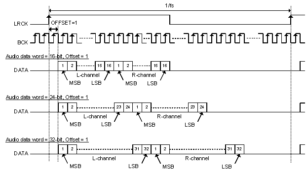
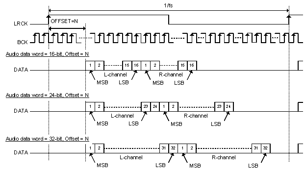
8.3.2.3 Zero Data Detect
The PCM514x has a zero-detect function. When the device detects the continuous zero data for both left and right channels, or separate channels, Analog mutes are set to both OUTL and OUTR, or separate OUTL and OUTR. These are controlled by Page 0, Register 65, D(2:1) as shown in Table 5.
Continuous Zero data cycles are counted by LRCK, and the threshold of decision for analog mute can be set by Page 0, Register 59, D(6:4) for L-ch, and D(2:0) for Rch as shown in Table 6. Default values are 0 for both channels.
In Hardware mode, the device uses default values. By default, Both L-ch and R-ch have to be zero data for zero data detection to begin the muting process etc.
Table 5. Zero Data Detection Mode
| ATMUTECTL | VALUE | FUNCTION |
|---|---|---|
| Bit : 2 | 0 | Independently L-ch or R-ch are zero data for zero data detection |
| 1 (Default) | Both L-ch and R-ch have to be zero data for zero data detection | |
| Bit : 1 | 0 | Zero detection and analog mute are disabled for R-ch |
| 1 (Default) | Zero detection analog mute are enabled for R-ch | |
| Bit : 0 | 0 | Zero detection analog mute are disabled for L-ch |
| 1 (Default) | Zero detection analog mute are enabled for L-ch |
Table 6. Zero Data Detection Time
| ATMUTETIML / ATMUTETIMR | NUMBER OF LRCKs | TIME AT 48 kHz |
|---|---|---|
| 0 0 0 | 1024 | 21 ms |
| 0 0 1 | 5120 | 106 ms |
| 0 1 0 | 10240 | 213 ms |
| 0 1 1 | 25600 | 533 ms |
| 1 0 0 | 51200 | 1.066 sec |
| 1 0 1 | 102400 | 2.133 sec |
| 1 1 0 | 256000 | 5.333 sec |
| 1 1 1 | 512000 | 10.66 sec |
8.3.3 XSMT Pin (Soft Mute / Soft Un-Mute)
An external digital host controls the PCM514x soft mute function by driving the XSMT pin with a specific minimum rise time (tr) and fall time (tf) for soft mute and soft un-mute. The PCM514x requires tr and tf times of less than 20 ns. In the majority of applications, this is no problem; however, traces with high capacitance may have issues.
When the XSMT pin is shifted from high to low (3.3 V to 0 V), a soft digital attenuation ramp begins. –1-dB attenuation is then applied every sample time from 0 dBFS to –∞. The soft attenuation ramp takes 104 samples.
When the XSMT pin is shifted from low to high (0 V to 3.3 V), a soft digital un-mute is started. 1-dB gain steps are applied every sample time from –∞ to 0 dBFS. The un-mute takes 104 samples.
In systems where XSMT is not required, it can be directly connected to AVDD.
8.3.4 Audio Processing
8.3.4.1 PCM514x Audio Processing Options
8.3.4.1.1 Overview
The PCM514x features a fully-programmable miniDSP core. The algorithms for the miniDSP must be loaded into the device after power up. The miniDSP has direct access to the digital stereo audio stream, offering the possibility for advanced DSP algorithms with very low group delay. The miniDSP can run up to 1024 instructions on every audio sample at a 48-kHz sample rate.
NOTE
At higher sampling frequencies, fewer instruction cycles are available. (For example, 512 instructions can be done in a 96-kHz frame.)
The PCM514x supports two different code sources. ROM based process flow (See the next section for how to select) and RAM based process flow. In program 31 (RAM based), different algorithms can be called from ROM - such as EQ, DRC and Zero Crossing volume control. Please see the PurePath Studio Development Environment for more details.
8.3.4.1.2 miniDSP Instruction Register
Registers on Page 152-169 are 25-bit instructions for the miniDSP engine. For details, see Table 53. 7 bits of Instr(32:25) in Base register +0 are reserved bits. 1 bit of Instr(24) - (LSB) in Base register +0 is MSB bit of 25 bit instruction. These instructions control miniDSP operation. When the fully programmable miniDSP mode is enabled and the DAC channel is powered up, the read and write access to these registers is disabled.
8.3.4.1.3 Digital Output
The PCM514x supports an SDOUT output. This can be selected within the process flow, and driven out of a GPIO pin selected in the register map (for example, Page 0 / Register 80). Users should note that the I2S output will be attenuated by 0.5 dB. A full scale (FS) output will actually be FS-0.5dB. This can be compensated for within the process flow using PurePath Studio. The I2S output can be a separate audio stream to the analog DAC output, allowing 2.1 and 2.2 systems to be implimented. By default, the SDOUT is not linked to the volume control registers on Page 0 / Register 60, 61, 62. However, it is possible to configure the SDOUT component in Purepath studio to mirror that register.
8.3.4.1.4 Software
Software development for the PCM514x is supported through TI's comprehensive PurePath ™Studio; a powerful, easy-to-use tool designed specifically to simplify software development on the PCM514x miniDSP audio platform.
Please visit the PCM514x product folder on www.ti.com to learn more about PurePath Console and the latest status on available, ready-to-use DSP algorithms.
8.3.4.2 Interpolation Filter
The PCM514x provides 4 types of interpolation filters, selectable by writing to Page 0, Register 43, D(4:0).
Additional RAM based Hybrid Flows can be implemented by selecting Program 31, and downloading instructions and coefficients to the device.
Table 7. ROM Preset Programs
| PROGRAM NUMBER | D(4:0) | DESCRIPTION | MINIMUM CYCLES |
|---|---|---|---|
| 0 | 0 0000 | Reserved | |
| 1 | 0 0001 | Normal x8/x4/x2/x1 Interpolation Filter(1) | 256 |
| 2 | 0 0010 | Low Latency x8/x4/x2/x1 Interpolation Filter(1) | 256 |
| 3 | 0 0011 | High Attenuation x8/x4/x2 Interpolation Filter(1) | 512 |
| 4 | 0 0100 | Reserved | |
| 5 | 0 0101 | Preset Process Flow | |
| 6 | 0 0110 | Reserved | |
| 7 | 0 0111 | Asymmetric FIR Interpolation Filter(1) | 512 |
| : | : | Reserved | |
| 31 | 1 1111 | RAM program / Hybrid Flows |
The PCM514x supports four sampling modes (single rate, dual rate, quad rate, and octal rate) which produce different oversampling rates (OSR) in the interpolation digital filter operation. These are shown in Table 8.
Table 8. Sampling Modes and Oversampling Rates
| SAMPLING MODE | SAMPLING FREQUENCY (fS) kHz | OVERSAMPLING RATE (OSR) |
|---|---|---|
| Single Rate | 8 | 8 or 16 |
| 16 | ||
| 32 | ||
| 44.1 | ||
| 48 | ||
| Dual Rate | 88.2 | 4 |
| 96 | ||
| Quad Rate | 176.4 | 2 |
| 192 | ||
| Octal Rate | 384 | 1 (Bypass) |
Table 9. Normal x8 Interpolation Filter, Single Rate
| PARAMETER | CONDITION | VALUE (TYP) | VALUE (MAX) | UNIT |
|---|---|---|---|---|
| Filter Gain Pass Band | 0 ……. 0.45 × fS | ±0.01 | dB | |
| Filter Gain Stop Band | 0.55 × fS ….. 7.455 × fS | -60 | dB | |
| Filter Group Delay | 20 × ts | S |
SPACE
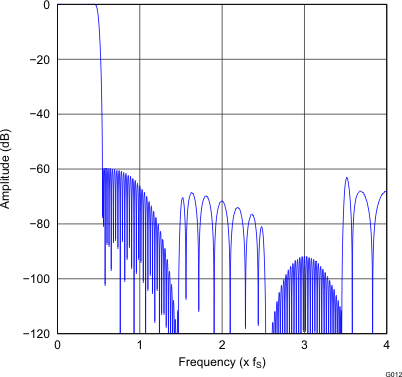 Figure 21. Normal x8 Interpolation Filter
 Frequency Response
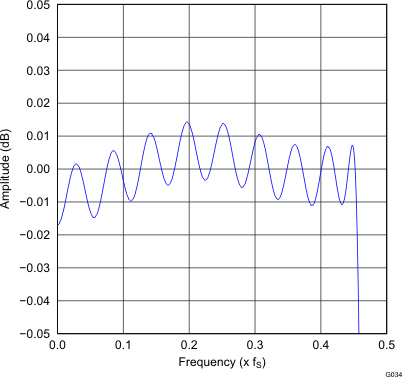 Figure 23. Normal x8 Interpolation Filter Passband Ripple
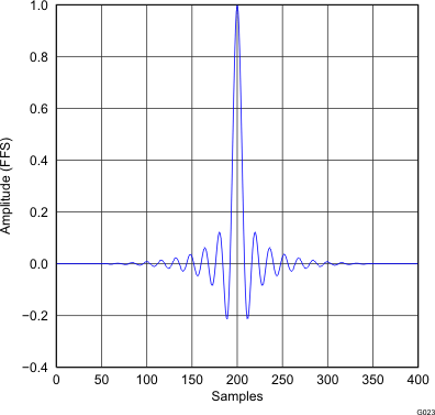 Figure 22. Normal x8 Interpolation Filter
 Impulse Response
Table 10. Normal x4 Interpolation Filter, Dual Rate
| PARAMETER | CONDITION | VALUE (TYP) | VALUE (MAX) | UNIT |
|---|---|---|---|---|
| Filter Gain Pass Band | 0 ……. 0.45 × fS | ±0.01 | dB | |
| Filter Gain Stop Band | 0.55 × fS ….. 3.455 × fS | -60 | dB | |
| Filter Group Delay | 20 × ts | S |
SPACE
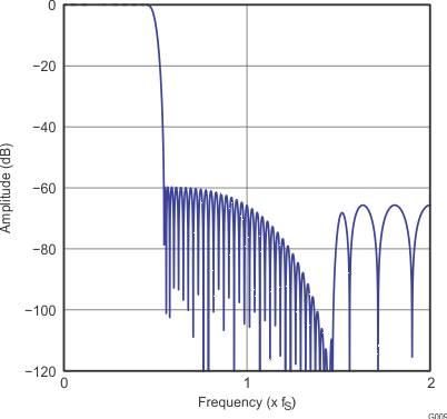 Figure 24. Normal x4 Interpolation Filter
 Frequency Response
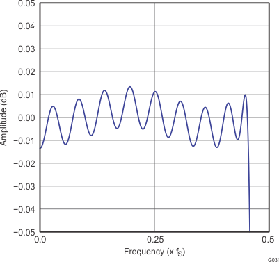 Figure 26. Normal x4 Interpolation Filter Passband Ripple
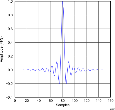 Figure 25. Normal x4 Interpolation Filter
 Impulse Response
Table 11. Normal x2 Interpolation Filter, Quad Rate
| PARAMETER | CONDITION | VALUE (TYP) | VALUE (MAX) | UNIT |
|---|---|---|---|---|
| Filter Gain Pass Band | 0 ……. 0.45 × fS | ±0.01 | dB | |
| Filter Gain Stop Band | 0.55 × fS ….. 1.455 × fS | -60 | dB | |
| Filter Group Delay | 20 × ts | S |
SPACE
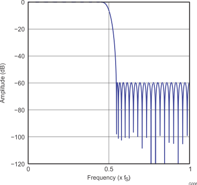 Figure 27. Normal x2 Interpolation Filter
 Frequency Response
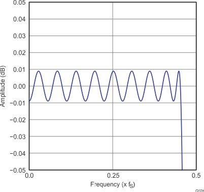 Figure 29. Normal x2 Interpolation Filter Passband Ripple
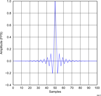 Figure 28. Normal x2 Interpolation Filter
 Impulse Response
Table 12. Low Latency x8 Interpolation Filter, Single Rate
| PARAMETER | CONDITION | VALUE (TYP) | VALUE (MAX) | UNIT |
|---|---|---|---|---|
| Filter Gain Pass Band | 0 ……. 0.45 × fS | ±0.001 | dB | |
| Filter Gain Stop Band | 0.55 × fS ….. 7.455 × fS | -52 | dB | |
| Filter Group Delay | 3.5 × ts | S |
SPACE
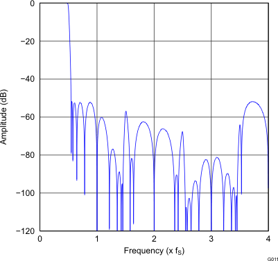 Figure 30. Low Latency x8 Interpolation Filter
 Frequency Response
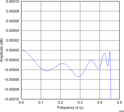 Figure 32. Low Latency x8 Interpolation Filter Passband Ripple
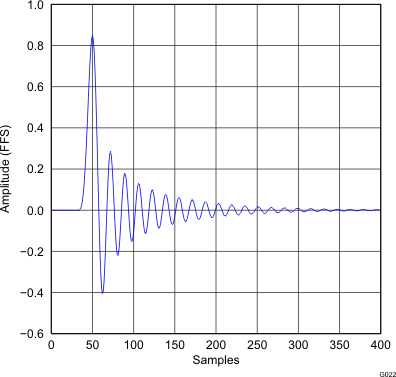 Figure 31. Low Latency x8 Interpolation Filter
 Impulse Response
Table 13. Low Latency x4 Interpolation Filter, Dual Rate
| PARAMETER | CONDITION | VALUE (TYP) | VALUE (MAX) | UNIT |
|---|---|---|---|---|
| Filter Gain Pass Band | 0 ……. 0.45 × fS | ±0.001 | dB | |
| Filter Gain Stop Band | 0.55 × fS ….. 3.455 × fS | -52 | dB | |
| Filter Group Delay | 3.5 × ts | S |
SPACE
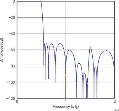 Figure 33. Low Latency x4 Interpolation Filter
 Frequency Response
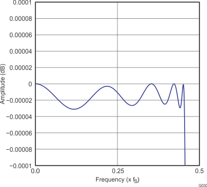 Figure 35. Low Latency x4 Interpolation Filter Passband Ripple
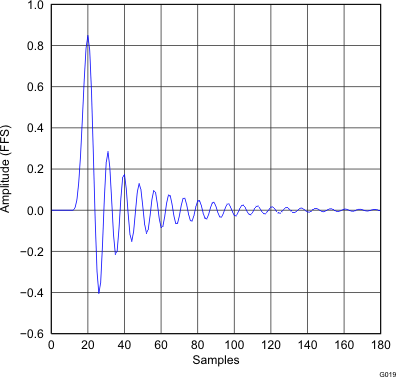 Figure 34. Low Latency x4 Interpolation Filter
 Impulse Response
Table 14. Low Latency ×2 Interpolation Filter, Quad Rate
| PARAMETER | CONDITION | VALUE (TYP) | VALUE (MAX) | UNIT |
|---|---|---|---|---|
| Filter Gain Pass Band | 0 ……. 0.45 × fS | ±0.001 | dB | |
| Filter Gain Stop Band | 0.55 × fS ….. 1.455 × fS | -52 | dB | |
| Filter Group Delay | 3.5 × ts | S |
SPACE
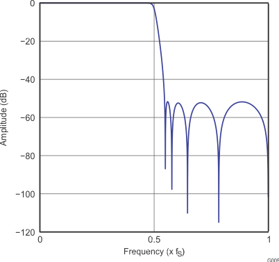 Figure 36. Low Latency x2 Interpolation Filter
 Frequency Response
 Figure 38. Low Latency x2 Interpolation Filter Passband Ripple
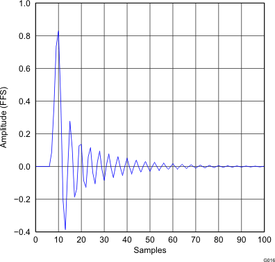 Figure 37. Low Latency x2 Interpolation Filter
 Impulse Response
Table 15. Asymmetric FIR x8 Interpolation Filter, Single Rate
| PARAMETER | CONDITION | VALUE (TYP) | VALUE (MAX) | UNIT |
|---|---|---|---|---|
| Filter Gain Pass Band | 0 ……. 0.40 × fS | ±0.05 | dB | |
| Filter Gain Stop Band | 0.72 × fS ….. 7.28 × fS | –50 | dB | |
| Filter Group Delay | 1.2 × ts | S |
SPACE
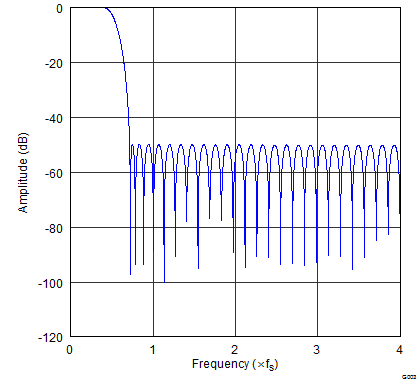 Figure 39. Asymmetric FIR x8 Interpolation Filter Frequency Response, Single Rate
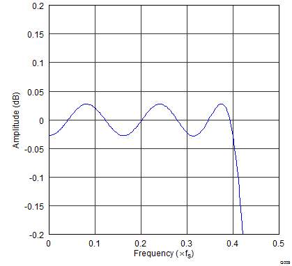 Figure 41. Asymmetric FIR x8 Interpolation Filter Passband Ripple, Single Rate
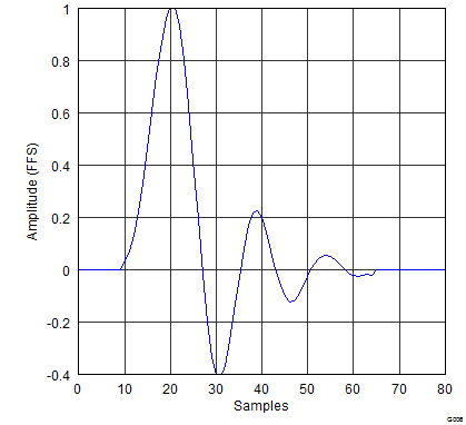 Figure 40. Asymmetric FIR x8 Interpolation Filter Impulse Response, Single Rate
Table 16. Asymmetric FIR x4 Interpolation Filter, Dual Rate
| PARAMETER | CONDITION | VALUE (TYP) | VALUE (MAX) | UNIT |
|---|---|---|---|---|
| Filter Gain Pass Band | 0 ……. 0.40 × fS | ±0.05 | dB | |
| Filter Gain Stop Band | 0.72 × fS ….. 3.28 × fS | –50 | dB | |
| Filter Group Delay | 1.2 × ts | S |
SPACE
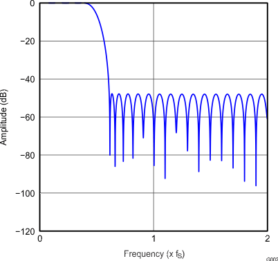 Figure 42. Asymmetric FIR x4 Interpolation Filter Frequency Response, Dual Rate
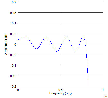 Figure 44. Asymmetric x4 Interpolation Filter Passband Ripple, Dual Rate
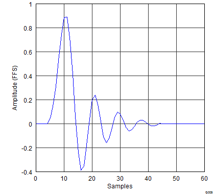 Figure 43. Asymmetric FIR x4 Interpolation Filter Impulse Response, Dual Rate
Table 17. Asymmetric FIR x2 Interpolation Filter, Quad Rate
| PARAMETER | CONDITION | VALUE (TYP) | VALUE (MAX) | UNIT |
|---|---|---|---|---|
| Filter Gain Pass Band | 0 ……. 0.40 × fS | ±0.05 | dB | |
| Filter Gain Stop Band | 0.72 × fS ….. 1.28 × fS | –50 | dB | |
| Filter Group Delay | 1.2 × ts | S |
SPACE
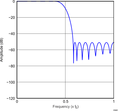 Figure 45. Asymmetric FIR x2 Interpolation Filter Frequency Response, Quad Rate
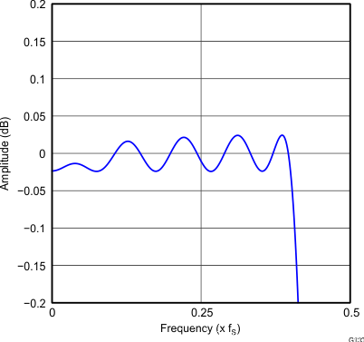 Figure 47. Asymmetric x2 Interpolation Filter Passband Ripple, Quad Rate
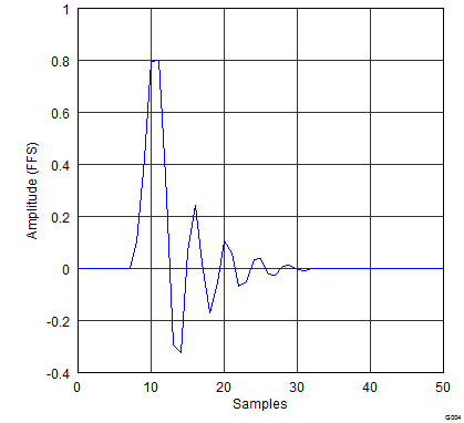 Figure 46. Asymmetric FIR x2 Interpolation Filter Impulse Response, Quad Rate
Table 18. High-Attentuation x8 Interpolation Filter, Single Rate
| PARAMETER | CONDITION | VALUE (TYP) | VALUE (MAX) | UNIT |
|---|---|---|---|---|
| Filter Gain Pass Band | 0 ……. 0.45 × fS | ±0.0005 | dB | |
| Filter Gain Stop Band | 0.55 × fS ….. 7.455 × fS | –100 | dB | |
| Filter Group Delay | 33.7 × tS | S |
SPACE
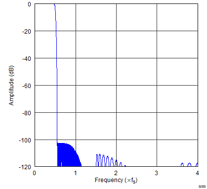 Figure 48. High-Attentuation x8 Interpolation Filter Frequency Response, Single Rate
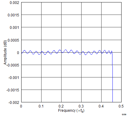 Figure 50. High-Attentuation x8 Interpolation Filter Passband Ripple, Single Rate
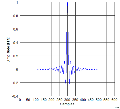 Figure 49. High-Attentuation x8 Interpolation Filter Impulse Response, Single Rate
Table 19. High-Attentuation x4 Interpolation Filter, Dual Rate
| PARAMETER | CONDITION | VALUE (TYP) | VALUE (MAX) | UNIT |
|---|---|---|---|---|
| Filter Gain Pass Band | 0 ……. 0.45 × fS | ±0.0005 | dB | |
| Filter Gain Stop Band | 0.55 × fS ….. 3.455 × fS | –100 | dB | |
| Filter Group Delay | 33.7 × tS | S |
SPACE
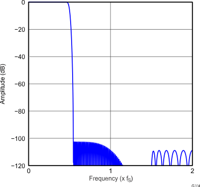 Figure 51. High-Attentuation x4 Interpolation Filter Frequency Response, Dual Rate
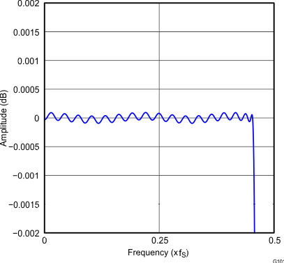 Figure 53. High-Attentuation x4 Interpolation Filter Passband Ripple, Dual Rate
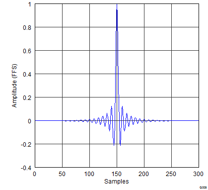 Figure 52. High-Attentuation x4 Interpolation Filter Impulse Response, Dual Rate
Table 20. High-Attentuation x2 Interpolation Filter, Quad Rate
| PARAMETER | CONDITION | VALUE (TYP) | VALUE (MAX) | UNIT |
|---|---|---|---|---|
| Filter Gain Pass Band | 0 ……. 0.45 × fS | ±0.0005 | dB | |
| Filter Gain Stop Band | 0.55 × fS ….. 1.455 × fS | –100 | dB | |
| Filter Group Delay | 33.7 × tS | S |
SPACE
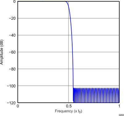 Figure 54. High-Attentuation x2 Interpolation Filter Frequency Response, Quad Rate
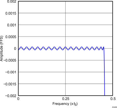 Figure 56. High-Attentuation x2 Interpolation Filter Passband Ripple, Quad Rate
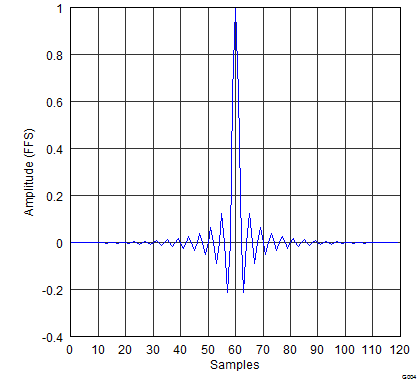 Figure 55. High-Attentuation x2 Interpolation Filter Impulse Response, Quad Rate
8.3.4.3 Fixed Audio Processing Flow (Program 5)
The PCM514x implements signal processing capabilities and interpolation filtering via processing blocks. These fixed processing blocks give users the choice of how much and what type of signal processing they may use and which interpolation filter is applied.
The signal processing blocks available are:
- Biquad filters
- Multiband DRC
- Mono mixer
- Stereo mixer
- Master volume
The addresses of the coefficients are fixed when selecting the fixed processing flow, however, if these components are used in the RAM source mode (Program 31) the registers for coefficients will change. Users can find more details in Purepath Studio.
NOTE
This process flow requires 1024 instruction cycles. Therefore, it will only function at sampling frequencies up to 48 kHz.
8.3.4.3.1 Processing Blocks – Detailed Descriptions
Figure 57 shows the fixed processing flow.
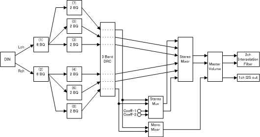 Figure 57. Preset Process Flow
Figure 58 shows a screen capture of PurePath Studio.
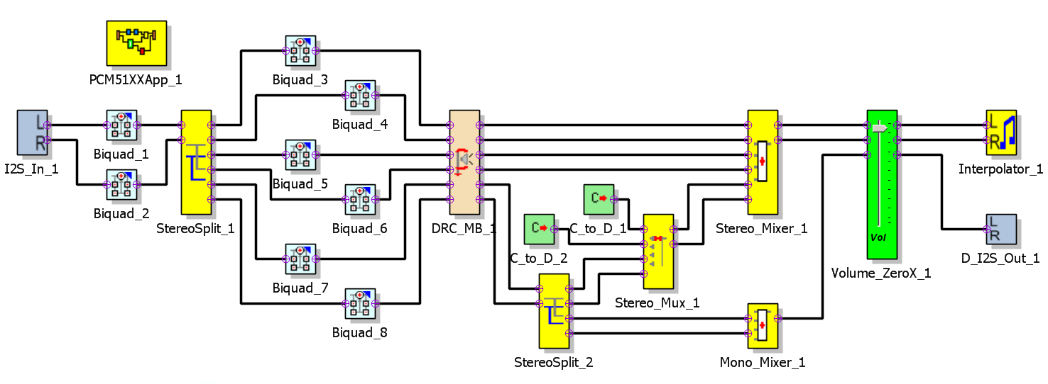 Figure 58. PurePath Studio Screen Capture
8.3.4.3.2 Biquad Section
The transfer function of each of the biquad filters is given by Equation 1.

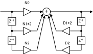 Figure 59. Biquad Block
Table 21. Biquad Filter Coefficients
| FILTER | CHANNEL | COEFFICIENT | REGISTER |
|---|---|---|---|
| BIQUAD (1) - 1 BIQUAD (2) - 1 | Lch, Rch |
N0 | C10 (Pg 44, Reg 48 ,49, 50, 51) |
| N1 | C11 (Pg 44, Reg 52, 53, 54, 55) | ||
| N2 | C12 (Pg 44, Reg 56, 57, 58, 59) | ||
| D1 | C13 (Pg 44, Reg 60, 61, 62, 63) | ||
| D2 | C14 (Pg 44, Reg 64, 65, 66, 67) | ||
| BIQUAD (1) - 2 BIQUAD (2) - 2 | Lch, Rch |
N0 | C15 (Pg 44, Reg 68, 69, 70, 71) |
| N1 | C16 (Pg 44, Reg 72, 73, 74, 75) | ||
| N2 | C17 (Pg 44, Reg 76, 77, 78, 79) | ||
| D1 | C18 (Pg 44, Reg 80, 81, 82, 83) | ||
| D2 | C19 (Pg 44, Reg 84, 85, 86, 87) | ||
| BIQUAD (1) - 3 BIQUAD (2) - 3 | Lch, Rch |
N0 | C20 (Pg 44, Reg 88, 89, 90, 91) |
| N1 | C21 (Pg 44, Reg 92, 93, 94, 95) | ||
| N2 | C22 (Pg 44, Reg 96, 97, 98, 99) | ||
| D1 | C23 (Pg 44, Reg 100, 101, 102, 103) | ||
| D2 | C24 (Pg 44, Reg 104, 105, 106, 107) | ||
| BIQUAD (1) - 4 BIQUAD (2) - 4 | Lch, Rch |
N0 | C25 (Pg 44, Reg 108, 109, 110, 111) |
| N1 | C26 (Pg 44, Reg 112, 113, 114, 115) | ||
| N2 | C27 (Pg 44, Reg 116, 117, 118, 119) | ||
| D1 | C28 (Pg 44, Reg 120, 121, 122, 123) | ||
| D2 | C29 (Pg 44, Reg 124, 125, 126, 127) | ||
| BIQUAD (1) - 5 BIQUAD (2) - 5 | Lch, Rch |
N0 | C30 (Pg 45, Reg 8, 9, 10, 11) |
| N1 | C31 (Pg 45, Reg 12, 13, 14, 15) | ||
| N2 | C32 (Pg 45, Reg 16, 17, 18, 19) | ||
| D1 | C33 (Pg 45, Reg 20, 21, 22, 23) | ||
| D2 | C34 (Pg 45, Reg 24, 25, 26, 27) | ||
| BIQUAD (1) - 6 BIQUAD (2) - 6 | Lch, Rch |
N0 | C35 (Pg 45, Reg 28, 29, 30, 31) |
| N1 | C36 (Pg 45, Reg 32, 33, 34, 35) | ||
| N2 | C37 (Pg 45, Reg 36, 37, 38, 39) | ||
| D1 | C38 (Pg 45, Reg 40, 41, 42, 43) | ||
| D2 | C39 (Pg 45, Reg 44, 45, 46, 47) | ||
| BIQUAD (3) - 1 BIQUAD (4) - 1 | Lch, Rch |
N0 | C40 (Pg 45, Reg 48, 49, 50, 51) |
| N1 | C41 (Pg 45, Reg 52, 53, 54, 55) | ||
| N2 | C42 (Pg 45, Reg 56, 57, 58, 59) | ||
| D1 | C43 (Pg 45, Reg 60, 61, 62, 63) | ||
| D2 | C44 (Pg 45, Reg 64, 65, 66, 67) | ||
| BIQUAD (3) - 2 BIQUAD (4) - 2 | Lch, Rch |
N0 | C45 (Pg 45, Reg 68, 69, 70, 71) |
| N1 | C46 (Pg 45, Reg 72, 73, 74, 75) | ||
| N2 | C47 (Pg 45, Reg 76, 77, 78, 79) | ||
| D1 | C48 (Pg 45, Reg 80, 81, 82, 83) | ||
| D2 | C49 (Pg 45, Reg 84, 85, 86, 87) | ||
| BIQUAD (5) - 1 BIQUAD (6) - 1 | Lch, Rch |
N0 | C50 (Pg 45, Reg 88, 89, 90, 91) |
| N1 | C51 (Pg 45, Reg 92, 93, 94, 95) | ||
| N2 | C52 (Pg 45, Reg 96, 97, 98, 99) | ||
| D1 | C53 (Pg 45, Reg 100, 101, 102, 103) | ||
| D2 | C54 (Pg 45, Reg 104, 105, 106, 107) | ||
| BIQUAD (5) - 2 BIQUAD (6) - 2 | Lch, Rch |
N0 | C55 (Pg 45, Reg 108, 109, 110, 111) |
| N1 | C56 (Pg 45, Reg 112, 113, 114, 115) | ||
| N2 | C57 (Pg 45, Reg 116, 117, 118, 119) | ||
| D1 | C58 (Pg 45, Reg 120, 121, 122, 123) | ||
| D2 | C59 (Pg 45, Reg 124, 125, 126, 127) | ||
| BIQUAD (7) - 1 BIQUAD (8) - 1 | Lch, Rch |
N0 | C60 (Pg 46, Reg 8, 9, 10, 11) |
| N1 | C61 (Pg 46, Reg 12, 13, 14, 15) | ||
| N2 | C62 (Pg 46, Reg 16, 17, 18, 19) | ||
| D1 | C63 (Pg 46, Reg 20, 21, 22, 23) | ||
| D2 | C64 (Pg 46, Reg 24, 25, 26, 27) | ||
| BIQUAD (7) - 2 BIQUAD (8) - 2 | Lch, Rch |
N0 | C65 (Pg 46, Reg 28, 29, 30, 31) |
| N1 | C66 (Pg 46, Reg 32, 33, 34, 35) | ||
| N2 | C67 (Pg 46, Reg 36, 37, 38, 39) | ||
| D1 | C68 (Pg 46, Reg 40, 41, 42, 43) | ||
| D2 | C69 (Pg 46, Reg 44, 45, 46, 47) |
8.3.4.3.3 Dynamic Range Compression
Dynamic range compression (DRC) improves the overall listening experience. Typical music signals are characterized by crest factors (the ratio of peak signal power to average signal power) of 12 dB or more. To avoid audible distortion due to clipping of peak signals, the gain of the DAC channel must be adjusted so as not to cause hard clipping. As a result, the low applied gain during nominal periods causes the perception that the signal is not loud enough. To overcome this problem, the DRC in the PCM514x continuously monitors the output of the DAC Digital Volume control to detect its power level with respect to 0-dB full-scale. When the power level is low, the DRC increases the input signal gain to make it sound louder, and reduces the gain during peaks to avoid hard clipping. The DRC enables louder audio during nominal periods with a clearer, more pleasant listening experience.
The 3-band DRC function applies DRC to 3 different mono/stereo signals with 3 different time constants. The same DRC curve is applied on all the signals, enabling a multi-band DRC solution. The underlying DRC algorithm is the same as that available with the DRC component in PurePath Studio. In this instance, the DRC gain acts on each signal in time-multiplexed order, for example, 1-2-3, 1-2-3, 1-2-3.
Table 22. DRC Coefficients
| COEFFICIENT | REGISTER |
|---|---|
| DRC_MB_1_DRC_1_DRCAE | C70 (Pg 46, Reg 48, 49, 50, 51) |
| DRC_MB_1_DRC_1_DRC1AE | C71 (Pg 46, Reg 52, 53, 54, 55) |
| DRC_MB_1_DRC_1_DRCAA | C72 (Pg 46, Reg 56, 57, 58, 59) |
| DRC_MB_1_DRC_1_DRC1AA | C73 (Pg 46, Reg 60, 61, 62, 63) |
| DRC_MB_1_DRC_1_DRCAD | C74 (Pg 46, Reg 64, 65, 66, 67) |
| DRC_MB_1_DRC_1_DRC1AD | C75 (Pg 46, Reg 68, 69, 70, 71) |
| DRC_MB_1_DRC_2_DRCAE | C76 (Pg 46, Reg 72, 73, 74, 75) |
| DRC_MB_1_DRC_2_DRC1AE | C77 (Pg 46, Reg 76, 77, 78, 79) |
| DRC_MB_1_DRC_2_DRCAA | C78 (Pg 46, Reg 80, 81, 82, 83) |
| DRC_MB_1_DRC_2_DRC1AA | C79 (Pg 46, Reg 84, 85, 86, 87) |
| DRC_MB_1_DRC_2_DRCAD | C80 (Pg 46, Reg 88, 89, 90, 91) |
| DRC_MB_1_DRC_2_DRC1AD | C81 (Pg 46, Reg 92, 93, 94, 95) |
| DRC_MB_1_DRC_3_DRCAE | C82 (Pg 46, Reg 96, 97, 98, 99) |
| DRC_MB_1_DRC_3_DRC1AE | C83 (Pg 46, Reg 100, 101, 102, 103) |
| DRC_MB_1_DRC_3_DRCAA | C84 (Pg 46, Reg 104, 105, 106, 107) |
| DRC_MB_1_DRC_3_DRC1AA | C85 (Pg 46, Reg 108, 109, 119, 111) |
| DRC_MB_1_DRC_3_DRCAD | C86 (Pg 46, Reg 112, 113, 114, 115) |
| DRC_MB_1_DRC_3_DRC1AD | C87 (Pg 46, Reg 116, 117, 118, 119) |
| DRC_MB_1_DRC_DRCK0 | C88 (Pg 46, Reg 120, 121, 122, 123) |
| DRC_MB_1_DRC_DRCK1 | C89 (Pg 46, Reg 124, 125, 126, 127) |
| DRC_MB_1_DRC_DRCK2 | C90 (Pg 47, Reg 8, 9, 10, 11) |
| DRC_MB_1_DRC_DRCMT1 | C91 (Pg 47, Reg 12, 13, 14, 15) |
| DRC_MB_1_DRC_DRCMT2 | C92 (Pg 47, Reg 16, 17, 18, 19) |
| DRC_MB_1_DRC_DRCOFF1 | C93 (Pg 47, Reg 20, 21, 22, 23) |
| DRC_MB_1_DRC_DRCOFF2 | C94 (Pg 47, Reg 24, 25, 26, 27) |
| DRC_MB_1_MinusOne_Q22 | C95 (Pg 47, Reg 28, 29, 30, 31) |
| DRC_MB_1_MinusTwo_Q22 | C96 (Pg 47, Reg 32, 33, 34, 35) |
| DRC_MB_1_One_M2 | C97 (Pg 47, Reg 36, 37, 38, 39) |
| DRC_MB_1_Zero | C98 (Pg 47, Reg 40, 41, 42, 43) |
| DRC_MB_1_En_dB | C99 (Pg 47, Reg 44, 45, 46, 47) |
| DRC_MB_1_Minus__Zero_dB | C100 (Pg 47, Reg 48, 49, 50, 51) |
| DRC_MB_1_60_dB | C101 (Pg 47, Reg 52, 53, 54, 55) |
| DRC_MB_1_Minus_60_dB | C102 (Pg 47, Reg 56, 57, 58, 59) |
| DRC_MB_1_12_dB | C103 (Pg 47, Reg 60, 61, 62, 63) |
| DRC_MB_1_Offset | C104 (Pg 47, Reg 64, 65, 66, 67) |
| DRC_MB_1_K | C105 (Pg 47, Reg 68, 69, 70, 71) |
| DRC_MB_1_x / DRC_MB_1_DRC | C106 (Pg 47, Reg 72, 73, 74, 75) |
| DRC_MB_1_48_dB | C107 (Pg 47, Reg 76, 77, 78, 79) |
| DRC_MB_1_Minus_48_dB | C108 (Pg 47, Reg 80, 81, 82, 83) |
| DRC_MB_1_c1_3 | C109 (Pg 47, Reg 84, 85, 86, 87) |
| DRC_MB_1_c1_2 | C110 (Pg 47, Reg 88, 89, 90, 91) |
| DRC_MB_1_c1_1 | C111 (Pg 47, Reg 92, 93, 94, 95) |
| DRC_MB_1_c1_0 | C112 (Pg 47, Reg 96, 97, 98, 99) |
| DRC_MB_1_O1_1 | C113 (Pg 47, Reg 100, 101, 102, 103) |
| DRC_MB_1_S1_1 | C114 (Pg 47, Reg 104, 105, 106, 107) |
| DRC_MB_1_O1_2 | C115 (Pg 47, Reg 108, 109, 119, 111) |
| DRC_MB_1_S1_2 | C116 (Pg 47, Reg 112, 113, 114, 115) |
| DRC_MB_1_O1_3 | C117 (Pg 47, Reg 116, 117, 118, 119) |
| DRC_MB_1_S1_3 | C118 (Pg 47, Reg 120, 121, 122, 123) |
| DRC_MB_1_One_1_Q17 | C119 (Pg 47, Reg 124, 125, 126, 127) |
| DRC_MB_1_Scale1 | C120 (Pg 48, Reg 8, 9, 10, 11) |
| DRC_MB_1_x1Coeff | C121 (Pg 48, Reg 12, 13, 14, 15) |
| DRC_MB_1_c2_3 | C122 (Pg 48, Reg 16, 17, 18, 19) |
| DRC_MB_1_c2_2 | C123 (Pg 48, Reg 20, 21, 22, 23) |
| DRC_MB_1_c2_1 | C124 (Pg 48, Reg 24, 25, 26, 27) |
| DRC_MB_1_c2_0 | C125 (Pg 48, Reg 28, 29, 30, 31) |
| DRC_MB_1_O2_1 | C126 (Pg 48, Reg 32, 33, 34, 35) |
| DRC_MB_1_S2_1 | C127 (Pg 48, Reg 36, 37, 38, 39) |
| DRC_MB_1_O2_2 | C128 (Pg 48, Reg 40, 41, 42, 43) |
| DRC_MB_1_S2_2 | C129 (Pg 48, Reg 44, 45, 46, 47) |
| DRC_MB_1_O2_3 | C130 (Pg 48, Reg 48, 49, 50, 51) |
| DRC_MB_1_S2_3 | C131 (Pg 48, Reg 52, 53, 54, 55) |
| DRC_MB_1_One_2_Q17 | C132 (Pg 48, Reg 56, 57, 58, 59) |
| DRC_MB_1_Scale2 | C133 (Pg 48, Reg 60, 61, 62, 63) |
| DRC_MB_1_x2Coeff | C134 (Pg 48, Reg 64, 65, 66, 67) |
| DRC_MB_1_R1_1 | C135 (Pg 48, Reg 68, 69, 70, 71) |
| DRC_MB_1_R1_2 | C136 (Pg 48, Reg 72, 73, 74, 75) |
| DRC_MB_1_R2_1 | C137 (Pg 48, Reg 76, 77, 78, 79) |
| DRC_MB_1_R2_2 | C138 (Pg 48, Reg 80, 81, 82, 83) |
| DRC_MB_1_Band1_GainC | C139 (Pg 48, Reg 84, 85, 86, 87) |
| DRC_MB_1_Band2_GainC | C140 (Pg 48, Reg 88, 89, 90, 91) |
| DRC_MB_1_Band3_GainC | C141 (Pg 48, Reg 92, 93, 94, 95) |
| DRC_MB_1_MinusOne_M1 | C142 (Pg 48, Reg 96, 97, 98, 99) |
| DRC_MB_1_One_M1 | C143 (Pg 48, Reg 100, 101, 102, 103) |
| DRC_MB_1_Band1_GainE | C144 (Pg 48, Reg 104, 105, 106, 107) |
| DRC_MB_1_Band2_GainE | C145 (Pg 48, Reg 108, 109, 110, 111) |
| DRC_MB_1_Band3_GainE | C146 (Pg 48, Reg 112, 113, 114, 115) |
| DRC_MB_1_minus_One_M2 | C147 (Pg 48, Reg 116, 117, 118, 119) |
8.3.4.3.4 Stereo Mixer
Three stereo inputs are mixed into one stereo output with input signal gain given by Equation 2.

where
- i=1:2,3
Figure 60 and Table 23 show the stereo mixer operation.
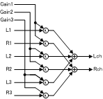 Figure 60. Stereo Mixer Block
Table 23. Stereo Mixer Coefficients
| COEFFICIENT | REGISTER |
|---|---|
| Stereo_Mixer_1_MixGain1 | C148 (Pg 48, Reg 120, 121, 122, 123) |
| Stereo_Mixer_1_MixGain2 | C149 (Pg 48, Reg 124, 125, 126, 127) |
| Stereo_Mixer_1_MixGain3 | C150 (Pg 49, Reg 8, 9, 10, 11) |
8.3.4.3.5 Stereo Multiplexer
The Stereo Multiplexer selects one or two from 4 stereo input channels.
 Figure 61. Stereo Multiplexer Block
Table 24. Stereo Multiplexer Select Coefficient
| COEFFICIENT | REGISTER |
|---|---|
| Stereo_Mux_1_MuxSelect | C152 (Pg 49, Reg 16, 17, 18, 19) |
Table 25. Stereo Multiplexer Input Coefficient
| COEFFICIENT | REGISTER |
|---|---|
| C_to_D_1_Coefval C_to_D_2_Coefval |
C153 (Pg 49, Reg 20, 21, 22, 23) |
8.3.4.3.6 Mono Mixer
The Mono Mixer computes a weighted sum of 2 input channels and produces an output.
 Figure 62. Mono Mixer Block
Table 26. Mono Mixer Coefficients
| COEFFICIENT | REGISTER |
|---|---|
| Mono_Mixer_1_MixGain1 | C154 (Pg 49, Reg 24, 25, 26, 27) |
| Mono_Mixer_1_MixGain2 | C155 (Pg 49, Reg 28, 29, 30, 31) |
8.3.4.3.7 Master Volume Control
The Master Volume controls the volume using a linear ramp and zero crossing detection for transitions.
Table 27. Mono Mixer Coefficients
| COEFFICIENT | REGISTER |
|---|---|
| Volume_ZeroX_1_volcmd | C158 (Pg 49, Reg 40, 41, 42, 43) |
| Volume_ZeroX_1_volout | C159 (Pg 49, Reg 44, 45, 46, 47) |
| Volume_ZeroX_1_volout_loudness | C160 (Pg 49, Reg 48, 49, 50, 51) |
| Volume_ZeroX_1_MinusOne_M2 | C161 (Pg 49, Reg 52, 53, 54, 55) |
| Volume_ZeroX_1_workingval_1_pre_CRAM | C162 (Pg 49, Reg 56, 57, 58, 59) |
| Volume_ZeroX_1_volout_pre1 | C163 (Pg 49, Reg 60, 61, 62, 63) |
| Volume_ZeroX_1_workingval_2_pre_CRAM | C164 (Pg 49, Reg 64, 65, 66, 67) |
| Volume_ZeroX_1_volout_pre2 | C165 (Pg 49, Reg 68, 69, 70, 71) |
| Volume_ZeroX_1_workingval_3_pre_CRAM | C166 (Pg 49, Reg 72, 73, 74, 75) |
| Volume_ZeroX_1_volout_pre3 | C167 (Pg 49, Reg 76, 77, 78, 79) |
| Volume_ZeroX_1_One_M2 | C168 (Pg 49, Reg 80, 81, 82, 83) |
| Volume_ZeroX_1_Zero | C169 (Pg 49, Reg 84, 85, 86, 87) |
| MinusOne_Int | C170 (Pg 49, Reg 88, 89, 90, 91) |
| MinusOne_M1 | C171 (Pg 49, Reg 92, 93, 94, 95) |
| One_M2 | C172 (Pg 49, Reg 96, 97, 98, 99) |
| One_M1 | C173 (Pg 49, Reg 100, 101, 102, 103) |
| Zero | C174 (Pg 49, Reg 104, 105, 106, 107) |
8.3.4.3.8 Miscellaneous Coefficients
Table 28. Miscellaneous Coefficients
| COEFFICIENT | REGISTER |
|---|---|
| DRC_MB_1_DataBlock | C175 (Pg 49, Reg 108, 109, 110, 111) |
| DRC_MB_1_CoeffBlock | C176 (Pg 49, Reg 112, 113, 114, 115) |
| Volume_ZeroX_1_DataBlock | C177 (Pg 49, Reg 116, 117, 118, 119) |
| Volume_ZeroX_1_CoeffBlock | C178 (Pg 49, Reg 120, 121, 122, 123) |
| plus_one | C179 (Pg 49, Reg 124, 125, 126, 127) |
| ADD_OF_filter_in_L | C180 (Pg 50, Reg 8, 9, 10, 11) |
| ADD_OF_filter_in_R | C181 (Pg 50, Reg 12, 13, 14, 15) |
8.3.5 DAC Outputs
8.3.5.1 Analog Outputs
The PCM514x devices include a two-channel DAC, with single-ended outputs. The full-scale output voltage is 2.1Vrms with ground center output. A dc-coupled load is supported in addition to an ac-coupled load, if the load resistance conforms to the specification. The PCM514x DAC outputs on the OUTL and OUTR terminals have market-leading low out-of-band noise, which offer up to 20dB lower out-of-band noise compared with existing DAC technology.
Most applications require an external low-pass RC filter (470Ω + 2.2nF) to provide sufficient out-of-band noise rejection. This RC filter provides the added advantage of improved protection against ESD damage.
8.3.5.2 Recommended Output Filter for the PCM514x
The diagram in Figure 63 shows the recommended output filter for the PCM514x. The new PCM514x next-generation current segment architecture offers excellent out-of-band noise, making a traditional 20-kHz low pass filter a thing of the past.
The RC settings below offer a –3-dB filter point at 153 kHz (approximately), giving the DAC the ability to reproduce virtually all frequencies through to it’s maximum sampling rate of 384 kHz. A NP0/C0G type capacitor is strongly recommended for the shunt capacitor for lowest distortion.
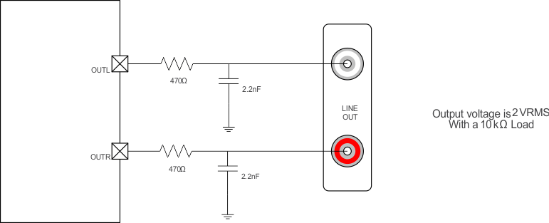 Figure 63. Recommended Output Lowpass Filter for 10-kΩ Operation
8.3.5.3 Choosing Between VREF and VCOM Modes
VREF mode is the default configuration. This mode allows full 2.1-Vrms signal output. As shown in Recommended Operating Conditions, the minimum AVDD to avoid clipping is 3.2 V.
VCOM mode allows setting a custom common-mode voltage when required by the application. This somewhat limits the output signal swing before clipping.
8.3.5.3.1 Voltage Reference and Output Levels
The PCM514x devices have an internal, fixed band-gap reference voltage, with default operation in VREF mode. No external decoupling capacitor is required for this mode.
The PCM514x devices can be operated with a common-mode voltage output (VCOM mode) at the VCOM pin by setting Page 1, Register 1, D(0) to 1. In this mode, an external decoupling capacitor is required.
When using this DAC in VREF mode, the output-signal voltage is independent of the power-supply voltage: The D/A conversion gain in VREF mode yields a 2.1-Vrms output voltage with a digital full-scale input. However, in VREF mode, an output waveform may clip due to the limitations that may be present in the analog power supply voltage. On the other hand, the full-scale output voltage in VCOM mode is proportional to the analog power supply AVDD (for example, (2.1 × AVDD / 3.3) Vrms).
8.3.5.3.2 Mode Switching Sequence, from VREF Mode to VCOM Mode
Following register setting sequence is recommended for changing VREF mode to VCOM mode.
| 1. | Page 0 / Register 2 | RQST = 1: Standby mode |
| 2. | Page 1 / Register 8 | RCMF = 1: Fast ramp up → on |
| 3. | Page 1 / Register 9 | VCPD = 0: VCOM is power on |
| 4. | Wait 3 ms with external capacitor = 1 µF | |
| 5. | Page 1 / Register 8 | RCMF = 0: Fast ramp up → off |
| 6. | Page 1 / Register 1 | OSEL = 1: VCOM mode |
| 7. | Page 0 / Register 2 | RQST = 0: Normal mode |
8.3.5.4 Digital Volume Control
A basic digital volume control with range from 24 dB to –103 dB and mute is available on each channels by Page 0, Resister 61, D(7:0) for L-ch and Register 62, D(7:0) for R-ch. These volume controls all have 0.5-dB step programmability over most gain and attenuation ranges. Table 29 lists the detailed gain versus programmed setting for this basic volume control. Volume can be changed for both L-ch and R-ch at the same time or independently by Page 0, Register 60, D(1:0). When D(1:0) set 00 (default), independent control is selected. When D(1:0) set 01, R-ch accords with L-ch volume. When D(1:0) set 10, L-ch accords with R-ch volume. To set D(1:0) to 11 is prohibited.
NOTE
This volume control is done externally to the miniDSP and only influences the analog DAC output. Any changes to the SDOUT data should be done in the miniDSP process flow.
Table 29. Digital Volume Control Settings
| GAIN SETTING | BINARY DATA | GAIN (dB) | COMMENTS |
|---|---|---|---|
| 0 | 0000-0000 | 24.0 | Positive maximum |
| 1 | 0000-0001 | 23.5 | |
| : | : | — | |
| 46 | 0010-1110 | 1.0 | |
| 47 | 0010-1111 | 0.5 | |
| 48 | 0011-0000 | 0.0 | No attenuation (default) |
| 49 | 0011-0001 | –0.5 | |
| 50 | 0011-0010 | –1.0 | |
| 51 | 0011-0011 | –1.5 | |
| : | : | — | |
| 253 | 1111-1101 | –102.5 | |
| 254 | 1111-1110 | –103 | Negative maximum |
| 255 | 1111-1111 | –∞ | Negative infinite (Mute) |
Ramp-up frequency and ramp-down frequency can be controlled by Page 0, Register 63, D(7:6) and D(3:2) as shown in Table 30. Also Ramp-up step and ramp-down step can be controlled by Page 0, Register 63 D(5:4) and D(1:0) as shown in Table 31.
Table 30. Ramp-Up or Down Frequency
| RAMP-UP SPEED | EVERY N fS | COMMENTS | RAMP-DOWN FREQUENCY | EVERY N fS | COMMENTS | |
|---|---|---|---|---|---|---|
| 00 | 1 | Default | 00 | 1 | Default | |
| 01 | 2 | 01 | 2 | |||
| 10 | 4 | 10 | 4 | |||
| 11 | Direct change | 11 | Direct change |
Table 31. Ramp-Up or Down Step
| RAMP-UP STEP | STEP dB | COMMENTS | RAMP-DOWN STEP | STEP dB | COMMENTS | |
|---|---|---|---|---|---|---|
| 00 | 4.0 | 00 | -4.0 | |||
| 01 | 2.0 | 01 | -2.0 | |||
| 10 | 1.0 | Default | 10 | -1.0 | Default | |
| 11 | 0.5 | 11 | -0.5 |
8.3.5.4.1 Emergency Ramp-Down
Digital volume emergency ramp-down by is provided for situations such as I2S clock error and power supply failure. Ramp-down speed is controlled by Page 0, Register 64, D(7:6). Ramp-down step can be controlled by Page 0 Register 64, D(5:4). Default is ramp-down by every fS cycle with –4-dB step.
8.3.5.5 Analog Gain Control
Analog gain control can be selected between 2-Vrms FS (0dB) or 1-Vrms FS (–6 dB). Gain is controlled through hardware by the AGNS pin, and through software (SPI/I2C), Page 1, Register 2, D4(L-ch) / D0(R-ch).
8.3.6 Reset and System Clock Functions
8.3.6.1 Clocking Overview
The PCM514x devices have flexible systems for clocking. Internally, the device requires a number of clocks, mostly at related clock rates to function correctly. All of these clocks can be derived from the serial audio interface in one form or another.
 Figure 64. Audio Flow with Respective Clocks
As shown in Figure 64 the data flows at the sample rate (fS). Once the data is brought into the serial audio interface, it gets processed, interpolated and modulated all the way to 128 × fS before arriving at the current segments for the final digital to analog conversion.
The clock tree is shown in Figure 65.
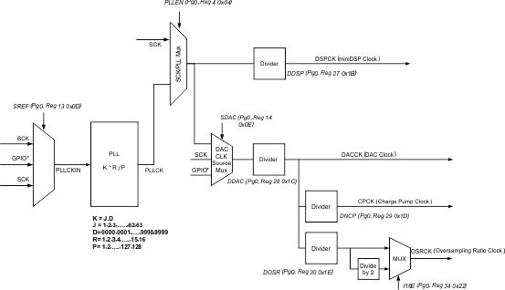 Figure 65. PCM514x Clock Distribution Tree
The serial audio interface typically has 4 connections: SCK (system master clock), BCK (bit clock), LRCK (left right word clock), and DIN (data). The device has an internal PLL that is used to take either SCK or BCK and create the higher rate clocks required by the interpolating processor and the DAC clock. This allows the device to operate with or without an external SCK.
In situations where the highest audio performance is required, it is suggested that the SCK is brought to the device, along with BCK and LRCK. The device should be configured so that the PLL is only providing a clock source to the miniDSP. By ensuring that the DACCK (DAC Clock) is being driven by the external SCK source, jitter evident in the PLL (in all PLLs) is kept out of the DAC, charge pump, and oversampling system.
Everything else should be a division of the incoming SCK. This is done by setting DAC CLK Source Mux (SDAC in Figure 65) to use SCK as a source, rather than the output of the SCK/PLL Mux. Code examples for this are available in SLASE12.
When the Auto Clock Configuration bit is set (Page 0/ Register 0x25), no additional clocks configuration is required. However, when setting custom PLL values and so forth, the target output rates should match those shown in the recommended PLL values of Table 132.
8.3.6.2 Clock Slave Mode With Master and System Clock (SCK) Input (4 Wire I2S)
The PCM514x requires a system clock to operate the digital interpolation filters and advanced segment DAC modulators. The system clock is applied at the SCK input and supports up to 50 MHz. The PCM514x system-clock detection circuit automatically senses the system-clock frequency. Common audio sampling frequencies in the bands of 8 kHz, 16 kHz, (32 kHz - 44.1 kHz - 48 kHz), (88.2kHz - 96kHz), (176.4 kHz - 192 kHz), and 384 kHz with ±4% tolerance are supported. Values in the parentheses are grouped when detected, (for example, 88.2 kHZ and 96 kHz are detected as double rate, and 32 kHz, 44.1 kHz and 48 kHz are detected as single rate.)
In the presence of a valid bit SCK, BCK and LRCK in software mode, the device will auto-configure the clock tree and PLL to drive the miniDSP as required.
The sampling frequency detector sets the clock for the digital filter, Delta Sigma Modulator (DSM) and the Negative Charge Pump (NCP) automatically. Table 32 shows examples of system clock frequencies for common audio sampling rates.
SCK rates that are not common to standard audio clocks, between 1 MHz and 50 MHz, are only supported in software mode by configuring various PLL and clock-divider registers. This programmability allows the device to become a clock master and drive the host serial port with LRCK and BCK, from a non-audio related clock (for example, using 12 MHz to generate 44.1 kHz [LRCK] and 2.8224 MHz [BCK]).
Table 32. System Master Clock Inputs for Audio Related Clocks
| SAMPLING FREQUENCY | SYSTEM CLOCK FREQUENCY (fSCK) (MHz) | |||||||||||
|---|---|---|---|---|---|---|---|---|---|---|---|---|
| 64 fS | 128 fS | 192 fS | 256 fS | 384 fS | 512 fS | 768 fS | 1024 fS | 1152 fS | 1536 fS | 2048 fS | 3072 fS | |
| 8 kHz | –(1) | 1.024(2) | 1.536(2) | 2.048 | 3.072 | 4.096 | 6.144 | 8.192 | 9.216 | 12.288 | 16.384 | 24.576 |
| 16 kHz | –(1) | 2.048(2) | 3.072(2) | 4.096 | 6.144 | 8.192 | 12.288 | 16.384 | 18.432 | 24.576 | 36.864 | 49.152 |
| 32 kHz | –(1) | 4.096(2) | 6.144(2) | 8.192 | 12.288 | 16.384 | 24.576 | 32.768 | 36.864 | 49.152 | –(1) | –(1) |
| 44.1 kHz | –(1) | 5.6488(2) | 8.4672(2) | 11.2896 | 16.9344 | 22.5792 | 33.8688 | 45.1584 | –(1) | –(1) | –(1) | –(1) |
| 48 kHz | –(1) | 6.144(2) | 9.216(2) | 12.288 | 18.432 | 24.576 | 36.864 | 49.152 | –(1) | –(1) | –(1) | –(1) |
| 88.2 kHz | –(1) | 11.2896(2) | 16.9344 | 22.5792 | 33.8688 | 45.1584 | –(1) | –(1) | –(1) | –(1) | –(1) | –(1) |
| 96 kHz | –(1) | 12.288(2) | 18.432 | 24.576 | 36.864 | 49.152 | –(1) | –(1) | –(1) | –(1) | –(1) | –(1) |
| 176.4 kHz | –(1) | 22.579 | 33.8688 | 45.1584 | –(1) | –(1) | –(1) | –(1) | –(1) | –(1) | –(1) | –(1) |
| 192 kHz | –(1) | 24.576 | 36.864 | 49.152 | –(1) | –(1) | –(1) | –(1) | –(1) | –(1) | –(1) | –(1) |
| 384 kHz | 24.576 | 49.152 | –(1) | –(1) | –(1) | –(1) | –(1) | –(1) | –(1) | –(1) | –(1) | –(1) |
See Timing Requirements: PCM Audio Data for clock timing requirements.
8.3.6.3 Clock Slave Mode With BCK PLL to Generate Internal Clocks (3-Wire PCM)
The system clock PLL mode allows designers to use a simple 3-wire I2S audio source. The 3-wire source reduces the need for a high frequency SCK, making PCB layout easier, and reduces high frequency electromagnetic interference.
In hardwired mode, the internal PLL is disabled as soon as an external SCK is supplied.
In hardwired mode, the device starts up expecting an external SCK input, but if BCK and LRCK start correctly while SCK remains at ground level for 16 successive LRCK periods, then the internal PLL starts, automatically generating an internal SCK from the BCK reference. Specific BCK rates are required to generate an appropriate master clock. Table 33 describes the minimum and maximum BCK per LRCK for the integrated PLL to automatically generate an internal SCK.
In software mode, the user must set all the PLL registers and clock divider registers for referencing BCK. See Clock Generation Using the PLL for more information. Recommended values can be found in Table 132.
Table 33. BCK Rates (MHz) by LRCK Sample Rate for PCM514x PLL Operation
| SAMPLE F (kHz) | BCK (fS) | |
|---|---|---|
| 32 | 64 | |
| 8 | – | – |
| 16 | – | 1.024 |
| 32 | 1.024 | 2.048 |
| 44.1 | 1.4112 | 2.8224 |
| 48 | 1.536 | 3.072 |
| 96 | 3.072 | 6.144 |
| 192 | 6.144 | 12.288 |
| 384 | 12.288 | 24.576 |
8.3.6.4 Clock Generation Using the PLL
The PCM514x supports a wide range of options to generate the required clocks for the DAC section as well as interface and other control blocks as shown in Figure 65.
The clocks for the PLL require a source reference clock. This clock is sourced as the incoming BCK or SCK. In software mode, a GPIO can also be used.
The source reference clock for the PLL reference clock is selected by programming the SRCREF value on Page 0, Register 13, D(6:4). The PCM514x provides several programmable clock dividers to achieve a variety of sampling rates for the DAC and clocks for the NCP, OSR, and the miniDSP. OSRCK for OSR must be set at 16 fS frequency by DOSR on Page0, Register 30, D(6:0). See Figure 65.
If PLL functionality is not required, set the PLLEN value on Page 0, Register 4, D(0) to 0. In this situation, an external SCK is required.
Table 34. PLL Configuration Registers
| CLOCK MULTIPLEXER | FUNCTION | BITS |
|---|---|---|
| SRCREF | PLL reference | Page 0, Register 13, D(6:4) |
| DIVIDER | FUNCTION | BITS |
| DDSP | miniDSP clock divider | Page 0, Register 27, D(6:0) |
| DACCK | DAC clock divider | Page 0, Register 28, D(6:0) |
| CPCK | NCP clock divider | Page 0, Register 29, D(6:0) |
| OSRCK | OSR clock divider | Page 0, Register 30, D(6:0) |
| DBCK | External BCK Div | Page 0, Register 32, D(6:0) |
| DLRK | External LRCK Div | Page 0, Register 33, D(7:0) |
8.3.6.5 PLL Calculation
The PCM514x has an on-chip PLL with fractional multiplication to generate the clock frequency needed by the audio DAC, Negative Charge Pump, Modulator and Digital Signal Processing blocks. The programmability of the PLL allows operation from a wide variety of clocks that may be available in the system. The PLL input (PLLCKIN) supports clock frequencies from 1 MHz to 50 MHz and is register programmable to enable generation of required sampling rates with fine precision.
The PLL is enabled by default. The PLL can be turned on by writing to Page 0, Register 4, D(0). When the PLL is enabled, the PLL output clock PLLCK is given by Equation 3.

where
- R = 1, 2, 3,4, ... , 15, 16
- J = 4,5,6, . . . 63, and D = 0000, 0001, 0002, . . . 9999
- K = [J value].[D value]
- P = 1, 2, 3, ... 15
R, J, D, and P are programmable. J is the integer portion of K (the numbers to the left of the decimal point), while D is the fractional portion of K (the numbers to the right of the decimal point, assuming four digits of precision).
8.3.6.5.1 Examples:
- If K = 8.5, then J = 8, D = 5000
- If K = 7.12, then J = 7, D = 1200
- If K = 14.03, then J = 14, D = 0300
- If K = 6.0004, then J = 6, D = 0004
When the PLL is enabled and D = 0000, the following conditions must be satisfied:
- 1 MHz ≤ ( PLLCKIN / P ) ≤ 20 MHz
- 64 MHz ≤ (PLLCKIN x K x R / P ) ≤ 100 MHz (in VREF mode)
- 72 MHz ≤ (PLLCKIN x K x R / P ) ≤ 86 MHz (in VCOM mode)
- 1 ≤ J ≤ 63
When the PLL is enabled and D ≠ 0000, the following conditions must be satisfied:
- 6.667 MHz ≤ PLLCLKIN / P ≤ 20 MHz
- 64 MHz ≤ (PLLCKIN x K x R / P ) ≤ 100 MHz (in VREF mode)
- 72 MHz ≤ (PLLCK IN x K x R / P ) ≤ 86 MHz (in VCOM mode)
- 4 ≤ J ≤ 11
- R = 1
When the PLL is enabled,
- fS = (PLLCLKIN × K × R) / (2048 × P)
- The value of N is selected so that fS × N = PLLCLKIN x K x R / P is in the allowable range.
Example: MCLK = 12 MHz and fS = 44.1 kHz, (N=2048)
Select P = 1, R = 1, K = 7.5264, which results in J = 7, D = 5264
Example: MCLK = 12 MHz and fS = 48.0 kHz, (N=2048)
Select P = 1, R = 1, K = 8.192, which results in J = 8, D = 1920
Values are written to the registers in Table 35.
8.3.6.5.1.1 Recommended PLL Settings
Recommended values for the PLL can be found after the register descriptions in this data sheet. Different values are defined based on the device configuration for VREF or VCOM mode.
Other configurations are possible, at your own risk.
Below are details of the register locations, as well as the nomenclature for the table of registers found at the end of this document.
Table 35. PLL Registers
| DIVIDER | FUNCTION | BITS |
|---|---|---|
| PLLE | PLL enable | Page 0, Register 4, D(0) |
| PPDV | PLL P | Page 0, Register 20, D(3:0) |
| PJDV | PLL J | Page 0, Register 21, D(5:0) |
| PDDV | PLL D | Page 0, Register 22, D(5:0) |
| Page 0, Register 23, D(7:0) | ||
| PRDV | PLL R | Page 0, Register 24, D(3:0) |
Table 36. PLL Configuration Recommendations
| COLUMN | DESCRIPTION |
|---|---|
| fS (kHz) | Sampling frequency |
| RSCK | Ratio between sampling frequency and SCK frequency (SCK frequency = RSCK × sampling frequency) |
| SCK (MHz) | System master clock frequency at SCK input (pin 20) |
| PLL VCO (MHz) | PLL VCO frequency as PLLCK in Figure 65 |
| P | One of the PLL coefficients in Equation 3 |
| PLL REF (MHz) | Internal reference clock frequency which is produced by SCK / P |
| M = K * R | The final PLL multiplication factor computed from K and R as described in Equation 3 |
| K = J.D | One of the PLL coefficients in Equation 3 |
| R | One of the PLL coefficients in Equation 3 |
| PLL fS | Ratio between fS and PLL VCO frequency (PLL VCO / fS) |
| DSP fS | Ratio between miniDSP operating clock rate and fS (PLL fS / NMAC) |
| NMAC | The miniDSP clock divider value in Table 34 |
| DSP CLK (MHz) | The miniDSP operating frequency as DSPCK in Figure 65 |
| MOD fS | Ratio between DAC operating clock frequency and fS (PLL fS / NDAC) |
| MOD f (kHz) | DAC operating frequency as DACCK in Figure 65 |
| NDAC | DAC clock divider value in Table 34 |
| DOSR | OSR clock divider value in Table 34 for generating OSRCK in Figure 65. DOSR must be chosen so that MOD fS / DOSR = 16 for correct operation. |
| NCP | NCP (negative charge pump) clock divider value in Table 34 |
| CP f | Negative charge pump clock frequency (fS × MOD fS / NCP) |
| % Error | Percentage of error between PLL VCO / PLL fS and fS (mismatch error).
|
8.3.6.6 Clock Master Mode from Audio Rate Master Clock
In Master Mode, the device generates bit clock (BCK) and left-right clock (LRCK) and outputs them on the appropriate pins. To configure the device in this mode, first put the device into reset, then use registers BCKO and LRKO (Pg 0, Reg 9 0x09). Then reset the LRCK and BCK divider counters using bits RBCK and RLRK (Pg 0, Reg 12 0x0C). Finally, exit reset.
An example of this is given in register programming examples in the PCM5242 data sheet (SLASE12.)
Figure 66 shows a simplified serial port clock tree for the device in master mode.
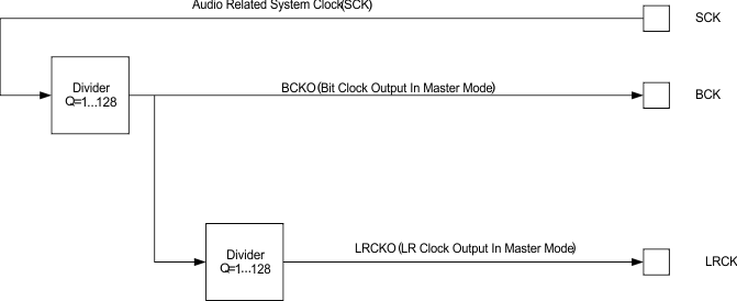 Figure 66. Simplified Clock Tree for SCK Sourced Master Mode
In master mode, SCK is an input and BCK/LRCK are outputs. BCK and LRCK are integer divisions of SCK. Master mode with a non-audio rate master clock source will require external GPIOs to use the PLL in standalone mode.
The PLL will also need to be configured to ensure that the onchip miniDSP processor can be driven at its maximum clock rate.
Register changes that need to be done include switching the device into master mode, and setting the divider ratio.
Here is an example of using 24.576 MCLK as a master clock source and driving the BCK and LRCK with integer dividers to create 48 kHz.
In this mode, the DAC section of the device is also running from the PLL output. While the PLL inside the PCM514x is one that has been specified to achieve the stated performance, using the SCK CMOS Oscillator source will have less jitter.
To switch the DAC clocks (SDAC in the Figure 65) the following registers should be modified.
- Clock Tree Flex Mode (Page 253, Registers 0x3F and 0x40)
- DAC and OSR Source Clock Register (Page 0, Reg 14) – set to 0x30 (SCK input, and OSR is set to whatever the DAC source is)
- The DAC clock divider should be 16 FS.
- 16 × 48 kHz = 768 kHz
- 24.576 MHz (SCK in) / 768 kHz = 32
- Therefor, divide ratio for register DDAC (Page 0, Reg 28 0x1C) should be set to 32. The may the register is mapped gives 0x00 = 1, so 32 must be converted to 0x1F.
An example configuration can be found in the PCM5242 data sheet (SLASE12).
8.3.6.7 Clock Master from a Non-Audio Rate Master Clock
The classic example here is running a 12-MHz Master clock for a 48-kHz sampling system. Given the clock tree for the device (shown in Figure 65), a non-audio clock rate cannot be brought into the SCK to the PLL in master mode. Therefore, the PLL source must be configured to be a GPIO pin, and the output brought back into another GPIO pin.
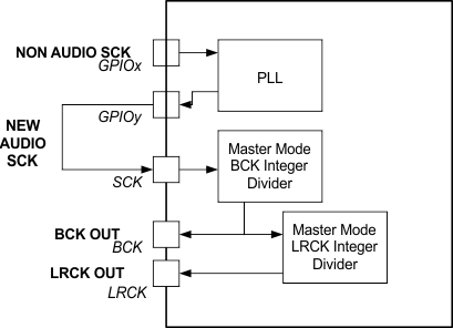 Figure 67. Application Diagram for Using Non-Audio Clock Sources to Generate Audio Clocks
The clock flow through the system is shown in Figure 67. The newly-generated SCK must be brought out of the device on a GPIO pin, then brought into the SCK pin for integer division to create BCK and LRCK outputs.
NOTE
Pullup resistors must be used on BCK and LRCK in this mode to ensure the device does not go into sleep mode.
A code example for configuring this mode is provided in the PCM5242 data sheet (SLASE12).
8.4 Device Functional Modes
8.4.1 Choosing a Control Mode
SPI Mode is selected by connecting MODE1 to DVDD. SPI Mode uses four signal lines and allows higher-speed full-duplex communication between the host and the PCM514x device.
I2C Mode is selected by connecting MODE1 to DGND and Mode2 to DVDD. I2C uses two signal lines for half-duplex communication, and is widely used in a variety of devices.
Hardware Control Mode is selected by connecting both MODE1 and MODE2 pins to DGND. Hardware control is useful in applications that do not require on-the-fly device-reconfiguration changes in operating features such as gain or filter latency selection.
See for a comparison of pin assignments for the 28-pin TSSOP.
8.4.1.1 Software Control
8.4.1.1.1 SPI Interface
The SPI interface is a 4-wire synchronous serial port which operates asynchronously to the serial audio interface and the system clock (SCK). The serial control interface is used to program and read the on-chip mode registers.
The control interface includes MISO (pin 24), MOSI (pin 11), MC (pin 12), and MS (pin 18). MISO (Master In Slave Out) is the serial data output, used to read back the values of the mode registers; MOSI (Master Out Slave In) is the serial data input, used to program the mode registers.
MC is the serial bit clock, used to shift data in and out of the control port by falling edge of MC, and MS is the mode control enable with LOW active, used to enable the internal mode register access. If feedback from the device is not required, the MISO pin can be assigned to GPIO1 by register control.
8.4.1.1.1.1 Register Read and Write Operation
All read/write operations for the serial control port use 16-bit data words. Figure 68 shows the control data word format. The most significant bit is the read/write bit. For write operations, the bit must be set to 0. For read operations, the bit must be set to 1. There are seven bits, labeled IDX[6:0], that hold the register index (or address) for the read and write operations. The least significant eight bits, D[7:0], contain the data to be written to, or the data that was read from, the register specified by IDX[6:0].
Figure 68 and Figure 69 show the functional timing diagram to write or read through the serial control port. MS is held at a logic-1 state until a register access. To start the register write or read cycle, set MS to logic 0. Sixteen clocks are then provided on MC, corresponding to the 16 bits of the control data word on MOSI and read-back data on MISO. After the eighth clock cycle has completed, the data from the indexed-mode control register appears on MISO during the read operation. After the sixteenth clock cycle has completed, the data is latched into the indexed-mode control register during the write operation. To write or read subsequent data, MS is set to logic 1 once (see tMHH in Figure 73).
 Figure 68. Control Data Word Format; MDI
NOTE
B8 is used for selection of Write or Read. Setting = 0 indicates a Write, while = 1 indicates a Read. Bits 15–9 are used for register address. Bits 7–0 are used for register data. Multiple-byte write or read (up to 8 bytes) is supported while MS is kept low. The address field becomes the initial address, automatically incrementing for each byte.
 Figure 69. Serial Control Format; Write, Single Byte
 Figure 70. Serial Control Format; Write, Multiple Byte
 Figure 71. Serial Control Format; Read
 Figure 72. Serial Control Format; Read, Multiple Byte
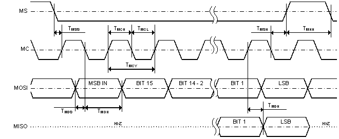 Figure 73. Control Interface Timing
Table 37. Control Interface Timing
| MIN | MAX | UNIT | ||
|---|---|---|---|---|
| tMCY | MC Pulse Cycle Time | 100 | ns | |
| tMCL | MC Low Level Time | 40 | ns | |
| tMCH | MC High Level Time | 40 | ns | |
| tMHH | MS High Level Time | 20 | ns | |
| tMSS | MS ↓ Edge to MC ↑ Edge | 30 | ns | |
| tMSH | MS Hold Time(1) | 30 | ns | |
| tMDH | MDI Hold Time | 15 | ns | |
| tMDS | MDI Set-up Time | 15 | ns | |
| tMOS | MC Rise Edge to MDO Stable | 20 | ns | |
8.4.1.1.2 I2C Interface
The PCM514x supports the I2C serial bus and the data transmission protocol for standard and fast mode as a slave device.
In I2C mode, the control terminals are changed as follows.
Table 38. I2C Pins and Functions
| SIGNAL | PIN | I/O | DESCRIPTION |
|---|---|---|---|
| SDA | 11 | I/O | I2C data |
| SCL | 12 | I | I2C clock |
| ADR2 | 16 | I | I2C address 2 |
| ADR1 | 24 | I | I2C address 1 |
8.4.1.1.2.1 Slave Address
Table 39. I2C Slave Address
| MSB | LSB | ||||||
| 1 | 0 | 0 | 1 | 1 | ADR2 | ADR1 | R/ W |
The PCM514x has 7 bits for its own slave address. The first five bits (MSBs) of the slave address are factory preset to 10011 (0x9x). The next two bits of the address byte are the device select bits which can be user-defined by the ADR1 and ADR0 terminals. A maximum of four devices can be connected on the same bus at one time. This gives a range of 0x98, 0x9A, 0x9C and 0x9E. Each PCM514x responds when it receives its own slave address.
8.4.1.1.2.2 Register Address Auto-Increment Mode
 Figure 74. Auto Increment Mode
Auto-increment mode allows multiple sequential register locations to be written to or read back in a single operation, and is especially useful for block write and read operations.
8.4.1.1.2.3 Packet Protocol
A master device must control packet protocol, which consists of start condition, slave address, read/write bit, data if write or acknowledge if read, and stop condition. The PCM514x supports only slave receivers and slave transmitters.
 Figure 75. Packet Protocol
Table 40. Write Operation - Basic I2C Framework
| Transmitter | M | M | M | S | M | S | M | S | S | M | |
| Data Type | St | slave address | R/ | ACK | DATA | ACK | DATA | ACK | ACK | Sp |
Table 41. Read Operation - Basic I2C Framework
| Transmitter | M | M | M | S | S | M | S | M | M | M | |
| Data Type | St | slave address | R/ | ACK | DATA | ACK | DATA | ACK | NACK | Sp |
M = Master Device; S = Slave Device; St = Start Condition; Sp = Stop Condition
8.4.1.1.2.4 Write Register
A master can write to any PCM514x registers using single or multiple accesses. The master sends a PCM514x slave address with a write bit, a register address with auto-increment bit, and the data. If auto-increment is enabled, the address is that of the starting register, followed by the data to be transferred. When the data is received properly, the index register is incremented by 1 automatically. When the index register reaches 0x7F, the next value is 0x0. Table 42 shows the write operation.
Table 42. Write Operation
| Transmitter | M | M | M | S | M | S | M | S | M | S | S | M | ||
| Data Type | St | slave addr | W | ACK | inc | reg addr | ACK | write data 1 | ACK | write data 2 | ACK | ACK | Sp | |
M = Master Device; S = Slave Device; St = Start Condition; Sp = Stop Condition; W = Write; ACK = Acknowledge
8.4.1.1.2.5 Read Register
A master can read the PCM514x register. The value of the register address is stored in an indirect index register in advance. The master sends a PCM514x slave address with a read bit after storing the register address. Then the PCM514x transfers the data which the index register points to. When auto-increment is enabled, the index register is incremented by 1 automatically. When the index register reaches 0x7F, the next value is 0x0. Table 43 shows the read operation.
Table 43. Read Operation
| Transmitter | M | M | M | S | M | S | M | M | M | S | S | M | M | M | ||
| Data Type | St | slave addr | W | ACK | inc | reg addr | ACK | Sr | slave addr | R | ACK | data | ACK | NACK | Sp | |
M = Master Device; S = Slave Device; St = Start Condition; Sr = Repeated Start Condition; Sp = Stop Condition; W = Write; R = Read; NACK = Not acknowledge
8.4.1.1.2.6 Timing Characteristics
 Figure 76. Register Access Timing
Table 44. I2C Bus Timing
| MIN | MAX | UNIT | |||
|---|---|---|---|---|---|
| fSCL | SCL clock frequency | Standard | 100 | kHz | |
| Fast | 400 | kHz | |||
| tBUF | Bus free time between a STOP and START condition | Standard | 4.7 | µs | |
| Fast | 1.3 | ||||
| tLOW | Low period of the SCL clock | Standard | 4.7 | µs | |
| Fast | 1.3 | ||||
| tHI | High period of the SCL clock | Standard | 4.0 | µs | |
| Fast | 600 | ns | |||
| tRS-SU | Setup time for (repeated)START condition | Standard | 4.7 | µs | |
| Fast | 600 | ns | |||
| tS-HD | Hold time for (repeated)START condition | Standard | 4.0 | µs | |
| tRS-HD | Fast | 600 | ns | ||
| tD-SU | Data setup time | Standard | 250 | ns | |
| Fast | 100 | ||||
| tD-HD | Data hold time | Standard | 0 | 900 | ns |
| Fast | 0 | 900 | |||
| tSCL-R | Rise time of SCL signal | Standard | 20 + 0.1CB | 1000 | ns |
| Fast | 20 + 0.1CB | 300 | |||
| tSCL-R1 | Rise time of SCL signal after a repeated START condition and after an acknowledge bit | Standard | 20 + 0.1CB | 1000 | ns |
| Fast | 20 + 0.1CB | 300 | |||
| tSCL-F | Fall time of SCL signal | Standard | 20 + 0.1CB | 1000 | ns |
| Fast | 20 + 0.1CB | 300 | |||
| tSDA-R | Rise time of SDA signal | Standard | 20 + 0.1CB | 1000 | ns |
| Fast | 20 + 0.1CB | 300 | |||
| tSDA-F | Fall time of SDA signal | Standard | 20 + 0.1CB | 1000 | ns |
| Fast | 20 + 0.1CB | 300 | |||
| tP-SU | Setup time for STOP condition | Standard | 4.0 | µs | |
| Fast | 600 | ns | |||
| CB | Capacitive load for SDA and SCL line | 400 | pF | ||
| tSP | Pulse width of spike suppressed | Fast | 50 | ns | |
| VNH | Noise margin at High level for each connected device (including hysteresis) | 0.2 × VDD | V | ||
8.4.2 VREF and VCOM Modes
See Choosing Between VREF and VCOM Modes for information on configuring these modes.
8.5 Programming
In software mode, the PCM514x can act as an I2S master, generating BCK and LRCK as outputs from the SCK input.
Table 45. I2S Master Mode Registers
| REGISTER | FUNCTION |
|---|---|
| Page0, Register 9, D(0), D(4), and D(5) | I2S Master mode select |
| Register 32, D(6:0) | BCK divider and LRCK divider |
| Register 33, D(7:0) |
9 Application and Implementation
NOTE
Information in the following applications sections is not part of the TI component specification, and TI does not warrant its accuracy or completeness. TI’s customers are responsible for determining suitability of components for their purposes. Customers should validate and test their design implementation to confirm system functionality.
9.1 Application Information
The PCM514x family is flexible, and this flexibility gives rise to a number of design questions that define the design requirements for a given application.
9.2 Typical Application
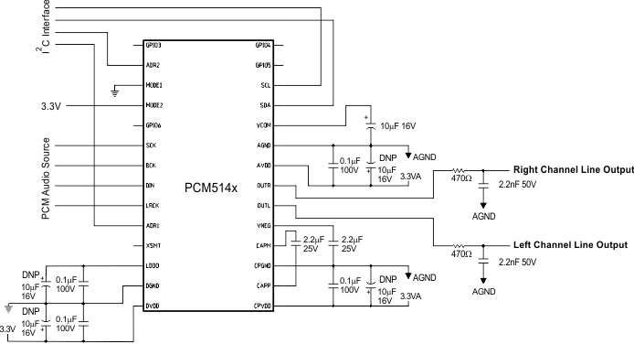 Figure 77. Simplified Schematic, Hardware-Controlled Subsystem
9.2.1 Design Requirements
- Single-ended 2.1-VRMS analog outputs
- 3-wire I2S interface (BCK PLL)
- Single 3.3-V supply
9.2.2 Detailed Design Procedure
- Clock and PLL setup (See Reset and System Clock Functions.) Ensure incoming BCK meets minimum requirements.
- XSMT pin setup for 12-V monitoring (See External Power Sense Undervoltage Protection Mode.)
- Single-supply 3.3-V operation (See Setting Digital Power Supplies and I/O Voltage Rails.)
9.2.3 Application Curve
 Figure 78. PCM5141A FFT Plot, DC to 20 kHz With a 1-kHz, –60-dBFS Input
10 Power Supply Recommendations
10.1 Power Supply Distribution and Requirements
The PCM514x devices are powered through the pins shown in Figure 79.
 Figure 79. Power Distribution Tree Within PCM514x
Table 46. Power Supply Pin Descriptions
| NAME | USAGE / DESCRIPTION |
|---|---|
| AVDD | Analog voltage supply; must be 3.3 V. This powers all analog circuitry that the DAC runs on. |
| DVDD | Digital voltage supply. This is used as the I/O voltage control and the input to the onchip LDO. |
| CPVDD | Charge Pump Voltage Supply - must be 3.3 V |
| LDOO | Output from the onchip LDO. Should be used with a 0.1-µF decoupling cap. Can be driven (used as power input) with a 1.8-V supply to bypass the onchip LDO for lower power consumption. |
| AGND | Analog ground |
| DGND | Digital ground |
10.2 Recommended Powerdown Sequence
Under certain conditions, the PCM514x devices can exhibit some pops on power down. Pops are caused by a device not having enough time to detect power loss and start the muting process.
The PCM514x devices have two auto-mute functions to mute the device upon power loss (intentional or unintentional).
10.2.1 XSMT = 0
When the XSMT pin is pulled low, the incoming PCM data is attenuated to 0, closely followed by a hard analog mute. This process takes 150 sample times (ts) + 0.2 ms.
Because this mute time is mainly dominated by the sampling frequency, systems sampling at 192 kHz will mute much faster than a 48-kHz system.
10.2.2 Clock Error Detect
When clock error is detected on the incoming data clock, the PCM514x devices switch to an internal oscillator, and continue to the drive the output, while attenuating the data from the last known value. Once this process is complete, the PCM514x outputs are hard muted to ground.
10.2.3 Planned Shutdown
These auto-muting processes can be manipulated by system designs to mute before power loss in the following ways:
- Assert XSMT low 150 tS + 0.2 ms before power is removed.
- Stop I2S clocks (SCK, BCK, LRCK) 3 ms before powerdown as shown in Figure 81.
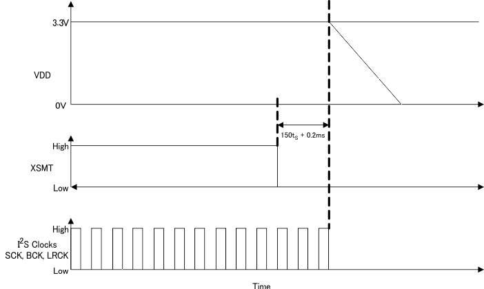 Figure 80. Assert XSMT
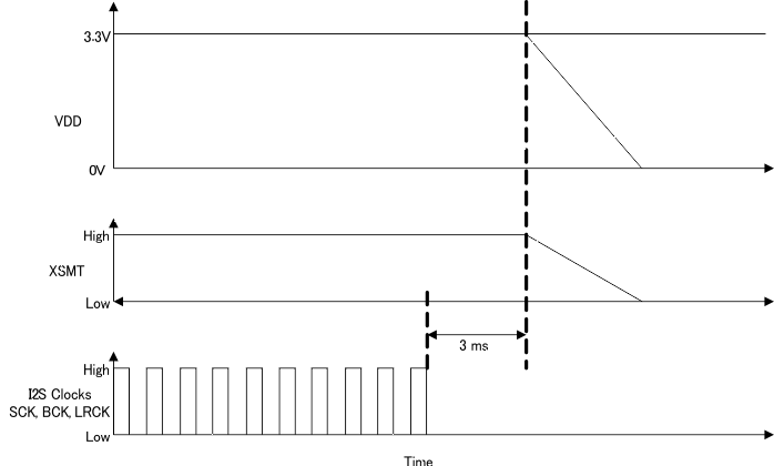 Figure 81. Stop I2C Clocks
10.2.4 Unplanned Shutdown
Many systems use a low-noise regulator to provide an AVDD 3.3-V supply for the DAC. The XSMT Pin can take advantage of such a feature to measure the pre-regulated output from the system SMPS to mute the output before the entire SMPS discharges. Figure 82 shows how to configure such a system to use the XSMT pin. The XSMT pin can also be used in parallel with a GPIO pin from the system microcontroller/DSP or power supply.
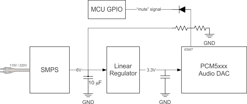 Figure 82. Using the XSMT Pin
10.3 External Power Sense Undervoltage Protection Mode
NOTE
External Power Sense Undervoltage Protection Mode is supported only when
DVDD = 3.3 V.
The XSMT pin can also be used to monitor a system voltage, such as the 24-VDC LCD TV backlight, or 12-VDC system supply using a voltage divider created with two resistors. (See Figure 83.)
- If the XSMT pin makes a transition from 1 to 0 over 6 ms or more, the device switches into external undervoltage protection mode. This mode uses two trigger levels:
- When the XSMT pin level reaches 2 V, soft mute process begins.
- When the XSMT pin level reaches 1.2 V, analog mute engages, regardless of digital audio level, and analog shutdown begins. (DAC and related circuitry powers down).
If XSMT is moved from 1 to 0 in 20 ns or less, then the device will interpret it as a digital controlled request to mute. It will perform a soft mute, then move to standby.
A timing diagram to show this is shown in Figure 84.
NOTE
The XSMT input pin voltage range is from –0.3 V to DVDD + 0.3 V. The ratio of external resistors must produce a voltage within this input range. Any increase in power supply (such as power supply positive noise or ripple) can pull the XSMT pin higher than DVDD + 0.3 V.
For example, if the PCM514x is monitoring a 12-V input, and dividing the voltage by 4, then the voltage at XSMT during ideal power supply conditions is 3.3 V. A voltage spike higher than 14.4 V causes a voltage greater than 3.6 V (DVDD + 0.3) on the XSMT pin, potentially damaging the device.
Providing the divider is set appropriately, any DC voltage can be monitored.
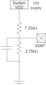 Figure 83. XSMT in External UVP Mode
 Figure 84. XSMT Timing for Undervoltage Protection
The trigger voltage values for the soft mute and hard mute are shown in Table 47. The range of values will vary from device to device, but typical thresholds are shown. XSMT should be set up to nominally be 3.3 V along with DVDD, but derived from a higher system power supply rail.
Table 47. Distribution of Voltage Thresholds
| MIN | TYP | MAX | UNIT | |
|---|---|---|---|---|
| Soft Mute Threshold Voltage | 2 | 2.2 | 0.9 × DVDD | V |
| Hard Mute Threshold Voltage | 0.1 × DVDD | 0.9 | 1.2 | V |
10.4 Power-On Reset Function
10.4.1 Power-On Reset, DVDD 3.3-V Supply
The PCM514x includes a power-on reset function, as shown in Figure 85. With VDD > 2.8 V, the power-on reset function is enabled. After the initialization period, the PCM514x is set to its default reset state. Analog output will begin ramping after valid data has been passing through the device for the given group delay given by the digital interpolation filter selected.
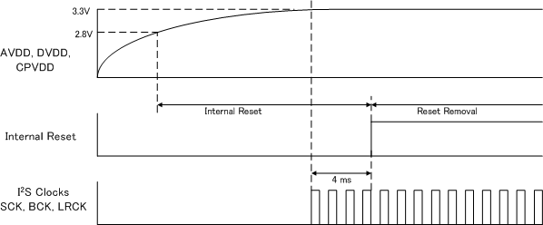 Figure 85. Power-On Reset Timing, DVDD = 3.3 V
10.4.2 Power-On Reset, DVDD 1.8-V Supply
The PCM514x includes a power-on reset function, as shown in Figure 86. With AVDD greater than approximately 2.8 V, CPVDD greater than approximately 2.8 V, and DVDD greater than approximately 1.5 V, the power-on reset function is enabled. After the initialization period, the PCM514x is set to its default reset state.
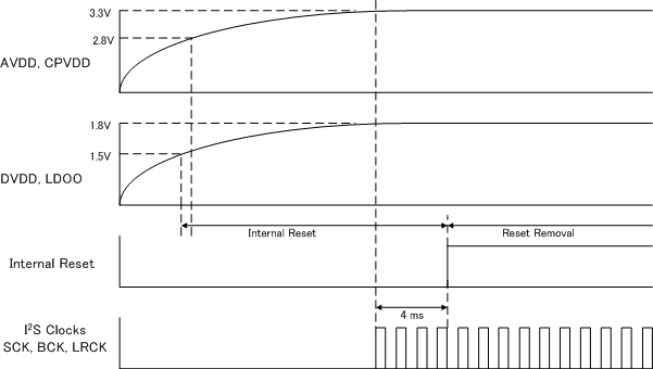 Figure 86. Power-On Reset Timing, DVDD = 1.8 V
10.5 PCM514x Power Modes
10.5.1 Setting Digital Power Supplies and I/O Voltage Rails
The internal digital core of the PCM514x devices run from a 1.8-V supply. This can be generated by the internal LDO, or by an external 1.8-V supply.
DVDD is used to set the I/O voltage, and to be used as the input to the onchip LDO that creates the 1.8 V required by the digital core.
For systems that require 3.3-V I/O support, but lower power consumption, DVDD should be connected to 3.3 V and LDOO can be connected to an external 1.8-V source. Doing so will disable the onchip LDO.
When setting I/O voltage to be 1.8 V, both DVDD and LDOO must be provided with an external 1.8-V supply.
10.5.2 Power Save Modes
The PCM514x devices offer two power-save modes: standby and power-down.
When a clock error (SCK, BCK, and LRCK) or clock halt is detected, the PCM514x device automatically enters standby mode. The DAC and line driver are also powered down.
When BCK and LRCK remain at a low level for more than 1 second, the PCM514x device automatically enters powerdown mode. Power-down mode disables the negative charge pump and bias/reference circuit, in addition to those disabled in standby mode.
When expected audio clocks (SCK, BCK, LRCK) are applied to the PCM514x device, or if BCK and LRCK start correctly while SCK remains at ground level for 16 successive LRCK periods, the device starts its powerup sequence automatically.
10.5.3 Power Save Parameter Programming
Table 48. Power Save Registers
| REGISTER | DESCRIPTION |
|---|---|
| Page 0, Register 2, D(4) | Software standby mode command |
| Page 0, Register 2, D(0) | Software power-down command |
| Page 0, Register 2, D(4) and D(0) | Software power-up sequence command (required after software standby or power-down) |
| Page 0, Register 44, D(2:0) | Detection time of BCK and LRCK halt |
11 Layout
11.1 Layout Guidelines
- The PCM514x family of devices are simple to layout. Most engineers use a shared common ground for an entire device. GND can consider AGND and DGND connected.
- Good system partitioning should keep digital clock and interface traces away from the analog outputs for highest analog performance. This reduces any high-speed clock return currents influencing the analog outputs.
- Power supply and charge pump decoupling capacitors should be placed as close as possible to the device.
- The top layer should be used for routing signals, whilst the bottom layer can be used for GND.
11.2 Layout Example
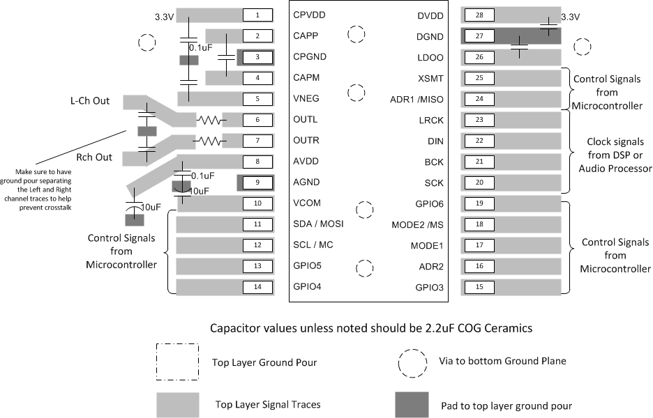
12 Register Maps
12.1 PCM514x Register Map
In any page, register 0 is the Page Select Register. The register value selects the Register Page from 0 to 255 for next read or write command.
Table 49. Register Map Overview
| REGISTER NUMBER | DESCRIPTION |
|---|---|
| Page 0 | |
| 0 | Page select register |
| 1 | Analog control register |
| 2 | Standby, Powerdown requests |
| 3 | Mute |
| 4 | PLL Lock Flag, PLL enable |
| 5 | Reserved |
| 6 | SPI MISO function select |
| 7 | De-emphasis enable, SDOUT select |
| 8 | GPIO enables |
| 9 | BCK, LRCLK configuration |
| 10 | DSP GPIO Input |
| 11 | Reserved |
| 12 | Master mode BCK, LRCLK reset |
| 13 | PLL clock source select |
| 14 - 19 | Reserved |
| 20 - 24 | PLL dividers |
| 25, 26 | Reserved |
| 27 | DSP clock divider |
| 28 | DAC clock divider |
| 29 | NCP clock divider |
| 30 | OSR clock divider |
| 31 | Reserved |
| 32, 33 | Master mode dividers |
| 34 | fS speed mode |
| 35, 36 | IDAC (number of DSP clock cycles available in one audio frame) |
| 37 | Ignore various errors |
| 38,39 | Reserved |
| 40, 41 | I2S configuration |
| 42 | DAC data path |
| 43 | DSP program selection |
| 44 | Clock missing detection period |
| 59 | Auto mute time |
| 60 - 64 | Digital volume |
| 65 | Auto mute |
| 75 - 79 | Reserved |
| 80 - 85 | GPIOn output selection |
| 86, 87 | GPIO control |
| 88, 89 | Reserved |
| 90 | DSP overflow |
| 91 - 94 | Sample rate status |
| 95 - 107 | Reserved |
| 108 | Analog mute monitor |
| 109 - 118 | Reserved |
| 119 | GPIO input |
| 120 | Auto Mute flags |
| 121 | Reserved |
| Page 1 | |
| 1 | Output amplitude type |
| 2 | Analog gain control |
| 3, 4 | Reserved |
| 5 | Undervoltage protection |
| 6 | Analog mute control |
| 7 | Analog gain boost |
| 8, 9 | VCOM configuration |
| Page 44 | |
| 1 | Coefficient memory (CRAM) control |
| Pages 44 - 52 | Coefficient buffer - A (256 coeffs x 24 bits) : See Table 51 |
| Pages 62 - 70 | Coefficient buffer - B (256 coeffs x 24 bits) : See Table 52 |
| Pages 152 - 186 | Instruction buffer (1024 instruction x 25 bits), I512 - I1023 are reserved.: See Table 53 |
| Pages 187 - 252 | Reserved |
| Page 253 | |
| 63, 64 | Clock Flex Mode |
| Pages 254 - 255 | Reserved |
The PCM514x has a register map split into multiple pages. Pages 0 and 1 control of the DAC and other on-chip peripherals. Pages 44 through 52 are used for Coefficient A memory, while Pages 62-70 are coefficient B memory. Pages 152-186 contain the miniDSP instruction memory. Page 253 is where the Clock Flex Mode register is located.
Table 50. PCM514x Register Page Structure
| Page: | 0 | 1 | 2-43 | 44-52 | 53-61 | 62-70 | 71-151 | 152-186 | 187-252 | 253 | 254-255 |
| Func: | Control | Analog Control | Reserved | Coeffient A | Reserved | Coeffient B | Reserved | Instruction | Reserved | Clock Flex | Reserved |
| Desc: | General Control and Configuration | Analog Control | 256 24-bit coefficients, 30 coefficients per page, 4 registers per coefficient |
256 24-bit coefficients, 30 coefficients per page, 4 registers per coefficient |
1024 24-bit instructions, 30 instructions per page, 4 registers per instruction |
Clock Flex Mode |
Table 51. Coefficient Buffer-A Map
| COEFF NO | PAGE NO | BASE REGISTER | BASE REGISTER + 0 | BASE REGISTER + 1 | BASE REGISTER + 2 | BASE REGISTER + 3 |
|---|---|---|---|---|---|---|
| C0 | 44 | 8 | Coef(23:16) | Coef(15:8) | Coef(7:0) | Reserved. |
| C1 | 44 | 12 | Coef(23:16) | Coef(15:8) | Coef(7:0) | Reserved. |
| .. | .. | .. | .. | .. | .. | .. |
| C29 | 44 | 124 | Coef(23:16) | Coef(15:8) | Coef(7:0) | Reserved. |
| C30 | 45 | 8 | Coef(23:16) | Coef(15:8) | Coef(7:0) | Reserved. |
| .. | .. | .. | .. | .. | .. | .. |
| C59 | 45 | 124 | Coef(23:16) | Coef(15:8) | Coef(7:0) | Reserved. |
| C60 | 46 | 8 | Coef(23:16) | Coef(15:8) | Coef(7:0) | Reserved. |
| .. | .. | .. | .. | .. | .. | .. |
| C89 | 46 | 124 | Coef(23:16) | Coef(15:8) | Coef(7:0) | Reserved. |
| C90 | 47 | 8 | Coef(23:16) | Coef(15:8) | Coef(7:0) | Reserved. |
| .. | .. | .. | .. | .. | .. | .. |
| C119 | 47 | 124 | Coef(23:16) | Coef(15:8) | Coef(7:0) | Reserved. |
| C120 | 48 | 8 | Coef(23:16) | Coef(15:8) | Coef(7:0) | Reserved. |
| .. | .. | .. | .. | .. | .. | .. |
| C149 | 48 | 124 | Coef(23:16) | Coef(15:8) | Coef(7:0) | Reserved. |
| C150 | 49 | 8 | Coef(23:16) | Coef(15:8) | Coef(7:0) | Reserved. |
| .. | .. | .. | .. | .. | .. | .. |
| C179 | 49 | 124 | Coef(23:16) | Coef(15:8) | Coef(7:0) | Reserved. |
| C180 | 50 | 8 | Coef(23:16) | Coef(15:8) | Coef(7:0) | Reserved. |
| .. | .. | .. | .. | .. | .. | .. |
| C209 | 50 | 124 | Coef(23:16) | Coef(15:8) | Coef(7:0) | Reserved. |
| C210 | 51 | 8 | Coef(23:16) | Coef(15:8) | Coef(7:0) | Reserved. |
| .. | .. | .. | .. | .. | .. | .. |
| C239 | 51 | 124 | Coef(23:16) | Coef(15:8) | Coef(7:0) | Reserved. |
| C240 | 52 | 8 | Coef(23:16) | Coef(15:8) | Coef(7:0) | Reserved. |
| .. | .. | .. | .. | .. | .. | .. |
| C255 | 52 | 68 | Coef(23:16) | Coef(15:8) | Coef(7:0) | Reserved. |
Table 52. Coefficient Buffer-B Map
| COEFF NO | PAGE NO | BASE REGISTER | BASE REGISTER + 0 | BASE REGISTER + 1 | BASE REGISTER + 2 | BASE REGISTER + 3 |
|---|---|---|---|---|---|---|
| C0 | 62 | 8 | Coef(23:16) | Coef(15:8) | Coef(7:0) | Reserved. |
| C1 | 62 | 12 | Coef(23:16) | Coef(15:8) | Coef(7:0) | Reserved. |
| .. | .. | .. | .. | .. | .. | .. |
| C29 | 62 | 124 | Coef(23:16) | Coef(15:8) | Coef(7:0) | Reserved. |
| C30 | 63 | 8 | Coef(23:16) | Coef(15:8) | Coef(7:0) | Reserved. |
| .. | .. | .. | .. | .. | .. | .. |
| C59 | 63 | 124 | Coef(23:16) | Coef(15:8) | Coef(7:0) | Reserved. |
| C60 | 64 | 8 | Coef(23:16) | Coef(15:8) | Coef(7:0) | Reserved. |
| .. | .. | .. | .. | .. | .. | .. |
| C89 | 64 | 124 | Coef(23:16) | Coef(15:8) | Coef(7:0) | Reserved. |
| C90 | 65 | 8 | Coef(23:16) | Coef(15:8) | Coef(7:0) | Reserved. |
| .. | .. | .. | .. | .. | .. | .. |
| C119 | 65 | 124 | Coef(23:16) | Coef(15:8) | Coef(7:0) | Reserved. |
| C120 | 66 | 8 | Coef(23:16) | Coef(15:8) | Coef(7:0) | Reserved. |
| .. | .. | .. | .. | .. | .. | .. |
| C149 | 66 | 124 | Coef(23:16) | Coef(15:8) | Coef(7:0) | Reserved. |
| C150 | 67 | 8 | Coef(23:16) | Coef(15:8) | Coef(7:0) | Reserved. |
| .. | .. | .. | .. | .. | .. | .. |
| C179 | 67 | 124 | Coef(23:16) | Coef(15:8) | Coef(7:0) | Reserved. |
| C180 | 68 | 8 | Coef(23:16) | Coef(15:8) | Coef(7:0) | Reserved. |
| .. | .. | .. | .. | .. | .. | .. |
| C209 | 68 | 124 | Coef(23:16) | Coef(15:8) | Coef(7:0) | Reserved. |
| C210 | 69 | 8 | Coef(23:16) | Coef(15:8) | Coef(7:0) | Reserved. |
| .. | .. | .. | .. | .. | .. | .. |
| C239 | 69 | 124 | Coef(23:16) | Coef(15:8) | Coef(7:0) | Reserved. |
| C240 | 70 | 8 | Coef(23:16) | Coef(15:8) | Coef(7:0) | Reserved. |
| .. | .. | .. | .. | .. | .. | .. |
| C255 | 70 | 68 | Coef(23:16) | Coef(15:8) | Coef(7:0) | Reserved. |
Table 53. miniDSP Instruction Map
| COEFF NO | PAGE NO | BASE REGISTER | BASE REGISTER + 0 | BASE REGISTER + 1 | BASE REGISTER + 2 | BASE REGISTER + 3 |
|---|---|---|---|---|---|---|
| I0 | 152 | 8 | Instr(31:24) | Instr(23:16) | Instr(15:8) | Instr(7:0) |
| I1 | 152 | 12 | Instr(31:24) | Instr(23:16) | Instr(15:8) | Instr(7:0) |
| .. | .. | .. | .. | .. | .. | .. |
| I29 | 152 | 124 | Instr(31:24) | Instr(23:16) | Instr(15:8) | Instr(7:0) |
| I30 | 153 | 8 | Instr(31:24) | Instr(23:16) | Instr(15:8) | Instr(7:0) |
| .. | .. | .. | .. | .. | .. | .. |
| I59 | 153 | 124 | Instr(31:24) | Instr(23:16) | Instr(15:8) | Instr(7:0) |
| I60 | 154 | 8 | Instr(31:24) | Instr(23:16) | Instr(15:8) | Instr(7:0) |
| .. | .. | .. | .. | .. | .. | .. |
| I89 | 154 | 124 | Instr(31:24) | Instr(23:16) | Instr(15:8) | Instr(7:0) |
| I90 | 155 | 8 | Instr(31:24) | Instr(23:16) | Instr(15:8) | Instr(7:0) |
| .. | .. | .. | .. | .. | .. | .. |
| I119 | 155 | 124 | Instr(31:24) | Instr(23:16) | Instr(15:8) | Instr(7:0) |
| I120 | 156 | 8 | Instr(31:24) | Instr(23:16) | Instr(15:8) | Instr(7:0) |
| .. | .. | .. | .. | .. | .. | .. |
| I149 | 156 | 124 | Instr(31:24) | Instr(23:16) | Instr(15:8) | Instr(7:0) |
| I150 | 157 | 8 | Instr(31:24) | Instr(23:16) | Instr(15:8) | Instr(7:0) |
| .. | .. | .. | .. | .. | .. | .. |
| I179 | 157 | 124 | Instr(31:24) | Instr(23:16) | Instr(15:8) | Instr(7:0) |
| I180 | 158 | 8 | Instr(31:24) | Instr(23:16) | Instr(15:8) | Instr(7:0) |
| .. | .. | .. | .. | .. | .. | .. |
| I209 | 158 | 124 | Instr(31:24) | Instr(23:16) | Instr(15:8) | Instr(7:0) |
| I210 | 159 | 8 | Instr(31:24) | Instr(23:16) | Instr(15:8) | Instr(7:0) |
| .. | .. | .. | .. | .. | .. | .. |
| I239 | 159 | 124 | Instr(31:24) | Instr(23:16) | Instr(15:8) | Instr(7:0) |
| I240 | 160 | 8 | Instr(31:24) | Instr(23:16) | Instr(15:8) | Instr(7:0) |
| .. | .. | .. | .. | .. | .. | .. |
| I269 | 160 | 124 | Instr(31:24) | Instr(23:16) | Instr(15:8) | Instr(7:0) |
| I270 | 161 | 8 | Instr(31:24) | Instr(23:16) | Instr(15:8) | Instr(7:0) |
| .. | .. | .. | .. | .. | .. | .. |
| I299 | 161 | 124 | Instr(31:24) | Instr(23:16) | Instr(15:8) | Instr(7:0) |
| I300 | 162 | 8 | Instr(31:24) | Instr(23:16) | Instr(15:8) | Instr(7:0) |
| .. | .. | .. | .. | .. | .. | .. |
| I329 | 162 | 124 | Instr(31:24) | Instr(23:16) | Instr(15:8) | Instr(7:0) |
| I330 | 163 | 8 | Instr(31:24) | Instr(23:16) | Instr(15:8) | Instr(7:0) |
| .. | .. | .. | .. | .. | .. | .. |
| I359 | 163 | 124 | Instr(31:24) | Instr(23:16) | Instr(15:8) | Instr(7:0) |
| I360 | 164 | 8 | Instr(31:24) | Instr(23:16) | Instr(15:8) | Instr(7:0) |
| .. | .. | .. | .. | .. | .. | .. |
| I389 | 164 | 124 | Instr(31:24) | Instr(23:16) | Instr(15:8) | Instr(7:0) |
| I390 | 165 | 8 | Instr(31:24) | Instr(23:16) | Instr(15:8) | Instr(7:0) |
| .. | .. | .. | .. | .. | .. | .. |
| I419 | 165 | 124 | Instr(31:24) | Instr(23:16) | Instr(15:8) | Instr(7:0) |
| I420 | 166 | 8 | Instr(31:24) | Instr(23:16) | Instr(15:8) | Instr(7:0) |
| .. | .. | .. | .. | .. | .. | .. |
| I449 | 166 | 124 | Instr(31:24) | Instr(23:16) | Instr(15:8) | Instr(7:0) |
| I450 | 167 | 8 | Instr(31:24) | Instr(23:16) | Instr(15:8) | Instr(7:0) |
| .. | .. | .. | .. | .. | .. | .. |
| I479 | 167 | 124 | Instr(31:24) | Instr(23:16) | Instr(15:8) | Instr(7:0) |
| I480 | 168 | 8 | Instr(31:24) | Instr(23:16) | Instr(15:8) | Instr(7:0) |
| .. | .. | .. | .. | .. | .. | .. |
| I509 | 168 | 124 | Instr(31:24) | Instr(23:16) | Instr(15:8) | Instr(7:0) |
| I510 | 169 | 8 | Instr(31:24) | Instr(23:16) | Instr(15:8) | Instr(7:0) |
| I511 | 169 | 12 | Instr(31:24) | Instr(23:16) | Instr(15:8) | Instr(7:0) |
| .. | .. | .. | .. | .. | .. | .. |
| I539 | 169 | 124 | Reserved. | Reserved. | Reserved. | Reserved. |
| I540 | 170 | 8 | Reserved. | Reserved. | Reserved. | Reserved. |
| .. | .. | .. | .. | .. | .. | .. |
| I569 | 170 | 124 | Reserved. | Reserved. | Reserved. | Reserved. |
| I570 | 171 | 8 | Reserved. | Reserved. | Reserved. | Reserved. |
| .. | .. | .. | .. | .. | .. | .. |
| I599 | 171 | 124 | Reserved. | Reserved. | Reserved. | Reserved. |
| I600 | 172 | 8 | Reserved. | Reserved. | Reserved. | Reserved. |
| .. | .. | .. | .. | .. | .. | .. |
| I629 | 172 | 124 | Reserved. | Reserved. | Reserved. | Reserved. |
| I630 | 173 | 8 | Reserved. | Reserved. | Reserved. | Reserved. |
| .. | .. | .. | .. | .. | .. | .. |
| I659 | 173 | 124 | Reserved. | Reserved. | Reserved. | Reserved. |
| I660 | 174 | 8 | Reserved. | Reserved. | Reserved. | Reserved. |
| .. | .. | .. | .. | .. | .. | .. |
| I689 | 174 | 124 | Reserved. | Reserved. | Reserved. | Reserved. |
| I690 | 175 | 8 | Reserved. | Reserved. | Reserved. | Reserved. |
| .. | .. | .. | .. | .. | .. | .. |
| I719 | 175 | 124 | Reserved. | Reserved. | Reserved. | Reserved. |
| I720 | 176 | 8 | Reserved. | Reserved. | Reserved. | Reserved. |
| .. | .. | .. | .. | .. | .. | .. |
| I749 | 176 | 124 | Reserved. | Reserved. | Reserved. | Reserved. |
| I750 | 177 | 8 | Reserved. | Reserved. | Reserved. | Reserved. |
| .. | .. | .. | .. | .. | .. | .. |
| I779 | 177 | 124 | Reserved. | Reserved. | Reserved. | Reserved. |
| I780 | 178 | 8 | Reserved. | Reserved. | Reserved. | Reserved. |
| .. | .. | .. | .. | .. | .. | .. |
| I809 | 178 | 124 | Reserved. | Reserved. | Reserved. | Reserved. |
| I810 | 179 | 8 | Reserved. | Reserved. | Reserved. | Reserved. |
| .. | .. | .. | .. | .. | .. | .. |
| I839 | 179 | 124 | Reserved. | Reserved. | Reserved. | Reserved. |
| I840 | 180 | 8 | Reserved. | Reserved. | Reserved. | Reserved. |
| .. | .. | .. | .. | .. | .. | .. |
| I869 | 180 | 124 | Reserved. | Reserved. | Reserved. | Reserved. |
| I870 | 181 | 8 | Reserved. | Reserved. | Reserved. | Reserved. |
| .. | .. | .. | .. | .. | .. | .. |
| I899 | 181 | 124 | Reserved. | Reserved. | Reserved. | Reserved. |
| I900 | 182 | 8 | Reserved. | Reserved. | Reserved. | Reserved. |
| .. | .. | .. | .. | .. | .. | .. |
| I929 | 182 | 124 | Reserved. | Reserved. | Reserved. | Reserved. |
| I930 | 183 | 8 | Reserved. | Reserved. | Reserved. | Reserved. |
| .. | .. | .. | .. | .. | .. | .. |
| I959 | 183 | 124 | Reserved. | Reserved. | Reserved. | Reserved. |
| I960 | 184 | 8 | Reserved. | Reserved. | Reserved. | Reserved. |
| .. | .. | .. | .. | .. | .. | .. |
| I989 | 184 | 124 | Reserved. | Reserved. | Reserved. | Reserved. |
| I990 | 185 | 8 | Reserved. | Reserved. | Reserved. | Reserved. |
| .. | .. | .. | .. | .. | .. | .. |
| I1019 | 185 | 124 | Reserved. | Reserved. | Reserved. | Reserved. |
| I1020 | 186 | 8 | Reserved. | Reserved. | Reserved. | Reserved. |
| .. | .. | .. | .. | .. | .. | .. |
| I1023 | 186 | 20 | Reserved. | Reserved. | Reserved. | Reserved. |
12.1.1 Detailed Register Descriptions
12.1.1.1 Register Map Summary
Table 54. Register Map Summary
| DEC | HEX | B7 | B6 | B5 | B4 | B3 | B2 | B1 | B0 |
|---|---|---|---|---|---|---|---|---|---|
| Page 0 | |||||||||
| 1 | 01 | RSV | RSV | RSV | RSTM | RSV | RSV | RSV | RSTR |
| 2 | 02 | RSV | RSV | RSV | RQST | RSV | RSV | RSV | RQPD |
| 3 | 03 | RSV | RSV | RSV | RQML | RSV | RSV | RSV | RQMR |
| 4 | 04 | RSV | RSV | RSV | PLCK | RSV | RSV | RSV | PLLE |
| 6 | 06 | RSV | RSV | RSV | RSV | RSV | RSV | FSMI1 | FSMI0 |
| 7 | 07 | RSV | RSV | RSV | DEMP | RSV | RSV | RSV | SDSL |
| 8 | 08 | RSV | RSV | G6OE | G5OE | G4OE | G3OE | G2OE | G1OE |
| 9 | 09 | RSV | RSV | BCKP | BCKO | RSV | RSV | RSV | LRKO |
| 10 | 0A | DSPG7 | DSPG6 | DSPG5 | DSPG4 | DSPG3 | DSPG2 | DSPG1 | DSPG0 |
| 12 | 0C | RSV | RSV | RSV | RSV | RSV | RSV | RBCK | RLRK |
| 13 | 0D | RSV | SREF2 | SREF1 | SREF0 | RSV | RSV | RSV | RSV |
| 14 | 0E | RSV | SDAC2 | SDAC1 | SDAC0 | RSV | RSV | RSV | RSV |
| 18 | 12 | RSV | RSV | RSV | RSV | RSV | GREF2 | GREF1 | GREF0 |
| 19 | 13 | RSV | RSV | RSV | RSV | RSV | RSV | RSV | RQSY |
| 20 | 14 | RSV | RSV | RSV | RSV | PPDV3 | PPDV2 | PPDV1 | PPDV0 |
| 21 | 15 | RSV | RSV | PJDV5 | PJDV4 | PJDV3 | PJDV2 | PJDV1 | PJDV0 |
| 22 | 16 | RSV | RSV | PDDV13 | PDDV12 | PDDV11 | PDDV10 | PDDV9 | PDDV8 |
| 23 | 17 | PDDV7 | PDDV6 | PDDV5 | PDDV4 | PDDV3 | PDDV2 | PDDV1 | PDDV0 |
| 24 | 18 | RSV | RSV | RSV | RSV | PRDV3 | PRDV2 | PRDV1 | PRDV0 |
| 27 | 1B | RSV | DDSP6 | DDSP5 | DDSP4 | DDSP3 | DDSP2 | DDSP1 | DDSP0 |
| 28 | 1C | RSV | DDAC6 | DDAC5 | DDAC4 | DDAC3 | DDAC2 | DDAC1 | DDAC0 |
| 29 | 1D | RSV | DNCP6 | DNCP5 | DNCP4 | DNCP3 | DNCP2 | DNCP1 | DNCP0 |
| 30 | 1E | RSV | DOSR6 | DOSR5 | DOSR4 | DOSR3 | DOSR2 | DOSR1 | DOSR0 |
| 32 | 20 | RSV | DBCK6 | DBCK5 | DBCK4 | DBCK3 | DBCK2 | DBCK1 | DBCK0 |
| 33 | 21 | DLRK7 | DLRK6 | DLRK5 | DLRK4 | DLRK3 | DLRK2 | DLRK1 | DLRK0 |
| 34 | 22 | RSV | RSV | RSV | I16E | RSV | RSV | FSSP1 | FSSP0 |
| 35 | 23 | IDAC15 | IDAC14 | IDAC13 | IDAC12 | IDAC11 | IDAC10 | IDAC9 | IDAC8 |
| 36 | 24 | IDAC7 | IDAC6 | IDAC5 | IDAC4 | IDAC3 | IDAC2 | IDAC1 | IDAC0 |
| 37 | 25 | RSV | IDFS | IDBK | IDSK | IDCH | IDCM | DCAS | IPLK |
| 40 | 28 | RSV | RSV | AFMT1 | AFMT0 | RSV | RSV | ALEN1 | ALEN0 |
| 41 | 29 | AOFS7 | AOFS6 | AOFS5 | AOFS4 | AOFS3 | AOFS2 | AOFS1 | AOFS0 |
| 42 | 2A | RSV | RSV | AUPL1 | AUPL0 | RSV | RSV | AUPR1 | AUPR0 |
| 43 | 2B | RSV | RSV | RSV | PSEL4 | PSEL3 | PSEL2 | PSEL1 | PSEL0 |
| 44 | 2C | RSV | RSV | RSV | RSV | RSV | CMDP2 | CMDP1 | CMDP0 |
| 59 | 3B | RSV | AMTL2 | AMTL1 | AMTL0 | RSV | AMTR2 | AMTR1 | AMTR0 |
| 60 | 3C | RSV | RSV | RSV | RSV | RSV | RSV | PCTL1 | PCTL0 |
| 61 | 3D | VOLL7 | VOLL6 | VOLL5 | VOLL4 | VOLL3 | VOLL2 | VOLL1 | VOLL0 |
| 62 | 3E | VOLR7 | VOLR6 | VOLR5 | VOLR4 | VOLR3 | VOLR2 | VOLR1 | VOLR0 |
| 63 | 3F | VNDF1 | VNDF0 | VNDS1 | VNDS0 | VNUF1 | VNUF0 | VNUS1 | VNUS0 |
| 64 | 40 | VEDF1 | VEDF0 | VEDS1 | VEDS0 | RSV | RSV | RSV | RSV |
| 65 | 41 | RSV | RSV | RSV | RSV | RSV | ACTL2 | AMLE1 | AMRE0 |
| 80 | 50 | RSV | RSV | RSV | G1SL4 | G1SL3 | G1SL2 | G1SL1 | G1SL0 |
| 81 | 51 | RSV | RSV | RSV | G2SL4 | G2SL3 | G2SL2 | G2SL1 | G2SL0 |
| 82 | 52 | RSV | RSV | RSV | G3SL4 | G3SL3 | G3SL2 | G3SL1 | G3SL0 |
| 83 | 53 | RSV | RSV | RSV | G4SL4 | G4SL3 | G4SL2 | G4SL1 | G4SL0 |
| 84 | 54 | RSV | RSV | RSV | G5SL4 | G5SL3 | G5SL2 | G5SL1 | G5SL0 |
| 85 | 55 | RSV | RSV | RSV | G6SL4 | G6SL3 | G6SL2 | G6SL1 | G6SL0 |
| 86 | 56 | RSV | RSV | GOUT5 | GOUT4 | GOUT3 | GOUT2 | GOUT1 | GOUT0 |
| 87 | 57 | RSV | RSV | GINV5 | GINV4 | GINV3 | GINV2 | GINV1 | GINV0 |
| 90 | 5A | RSV | RSV | RSV | L1OV | R1OV | L2OV | R2OV | SFOV |
| 91 | 5B | RSV | DTFS2 | DTFS1 | DTFS0 | DTSR3 | DTSR2 | DTSR1 | DTSR0 |
| 92 | 5C | RSV | RSV | RSV | RSV | RSV | RSV | RSV | DTBR8 |
| 93 | 5D | DTBR7 | DTBR6 | DTBR5 | DTBR4 | DTBR3 | DTBR2 | DTBR1 | DTBR0 |
| 94 | 5E | RSV | CDST | PLL-L | LrckBck | fS-SCKr | SCKval | BCKval | fSval |
| 95 | 5F | RSV | RSV | RSV | LTSH | RSV | CKMF | CSRF | CERF |
| 108 | 6C | RSV | RSV | RSV | RSV | RSV | RSV | AMLM | AMRM |
| 109 | 6D | RSV | RSV | RSV | SDTM | RSV | RSV | RSV | SHTM |
| 114 | 72 | RSV | RSV | RSV | RSV | RSV | RSV | MTST1 | MTST0 |
| 115 | 73 | RSV | RSV | RSV | RSV | RSV | RSV | FSMM1 | FSMM0 |
| 118 | 76 | BOTM | RSV | RSV | RSV | PSTM3 | PSTM2 | PSTM1 | PSTM0 |
| 119 | 77 | RSV | RSV | GPIN5 | GPIN4 | GPIN3 | GPIN2 | GPIN1 | RSV |
| 120 | 78 | RSV | RSV | RSV | AMFL | RSV | RSV | RSV | AMFR |
| 121 | 79 | RSV | RSV | RSV | RSV | RSV | RSV | RSV | DAMD |
| 122 | 7A | RSV | RSV | RSV | RSV | RSV | RSV | RSV | EIFM |
| 123 | 7B | RSV | G1MC2 | G1MC1 | G1MC0 | RSV | G2MC2 | G2MC1 | G2MC0 |
| 124 | 7C | RSV | G3MC2 | G3MC1 | G3MC0 | RSV | G4MC2 | G4MC1 | G4MC0 |
| 125 | 7D | RSV | G5MC2 | G5MC1 | G5MC0 | RSV | G6MC2 | G6MC1 | G6MC0 |
| Page 1 | |||||||||
| Dec | Hex | b7 | b6 | b5 | b4 | b3 | b2 | b1 | b0 |
| 1 | 01 | RSV | RSV | RSV | RSV | RSV | RSV | RSV | OSEL |
| 2 | 02 | RSV | RSV | RSV | LAGN | RSV | RSV | RSV | RAGN |
| 5 | 05 | RSV | RSV | RSV | RSV | RSV | RSV | UEPD | UIPD |
| 6 | 06 | RSV | RSV | RSV | RSV | RSV | RSV | RSV | AMCT |
| 7 | 07 | RSV | RSV | RSV | AGBL | RSV | RSV | RSV | AGBR |
| 8 | 08 | RSV | RSV | RSV | RSV | RSV | RSV | RSV | RCMF |
| 9 | 09 | RSV | RSV | RSV | RSV | RSV | RSV | RSV | VCPD |
| Page 44 | |||||||||
| Dec | Hex | b7 | b6 | b5 | b4 | b3 | b2 | b1 | b0 |
| 1 | 01 | RSV | RSV | RSV | RSV | ACRM | AMDC | ACRS | ACSW |
| Page 253 | |||||||||
| Dec | Hex | b7 | b6 | b5 | b4 | b3 | b2 | b1 | b0 |
| 63 | 3F | PLLFLEX17 | PLLFLEX16 | PLLFLEX15 | PLLFLEX14 | PLLFLEX13 | PLLFLEX12 | PLLFLEX11 | PLLFLEX10 |
| 64 | 40 | PLLFLEX27 | PLLFLEX26 | PLLFLEX25 | PLLFLEX24 | PLLFLEX23 | PLLFLEX22 | PLLFLEX21 | PLLFLEX20 |
12.1.1.2 Page 0 Registers
Table 55. Page 0 / Register 1
| Dec | Hex | b7 | b6 | b5 | b4 | b3 | b2 | b1 | b0 |
|---|---|---|---|---|---|---|---|---|---|
| 1 | 01 | RSV | RSV | RSV | RSTM | RSV | RSV | RSV | RSTR |
| Reset Value | 0 | 0 | |||||||
| RSV | Reserved | ||||||||
| Reserved. Do not access. | |||||||||
| RSTM | Reset Modules | ||||||||
| This bit resets the interpolation filter and the DAC modules. Since the DSP is also reset, the coeffient RAM content will also be cleared by the DSP. This bit is auto cleared and can be set only in standby mode. | |||||||||
| Default value: 0 | |||||||||
| 0: Normal | |||||||||
| 1: Reset modules | |||||||||
| RSTR | Reset Registers | ||||||||
| This bit resets the mode registers back to their initial values. The RAM content is not cleared, but the execution source will be back to ROM. This bit is auto cleared and must be set only when the DAC is in standby mode (resetting registers when the DAC is running is prohibited and not supported). | |||||||||
| Default value: 0 | |||||||||
| 0: Normal | |||||||||
| 1: Reset mode registers | |||||||||
Table 56. Page 0 / Register 2
| Dec | Hex | b7 | b6 | b5 | b4 | b3 | b2 | b1 | b0 |
|---|---|---|---|---|---|---|---|---|---|
| 2 | 02 | RSV | RSV | RSV | RQST | RSV | RSV | RSV | RQPD |
| Reset Value | 0 | 0 | |||||||
| RSV | Reserved | ||||||||
| Reserved. Do not access. | |||||||||
| RQST | Standby Request | ||||||||
| When this bit is set, the DAC will be forced into a system standby mode, which is also the mode the system enters in the case of clock errors. In this mode, most subsystems will be powered down but the charge pump and digital power supply. | |||||||||
| Default value: 0 | |||||||||
| 0: Normal operation | |||||||||
| 1: Standby mode | |||||||||
| RQPD | Powerdown Request | ||||||||
| When this bit is set, the DAC will be forced into powerdown mode, in which the power consumption would be minimum as the charge pump is also powered down. However, it will take longer to restart from this mode. This mode has higher precedence than the standby mode, that is, setting this bit along with bit 4 for standby mode will result in the DAC going into powerdown mode. | |||||||||
| Default value: 0 | |||||||||
| 0: Normal operation | |||||||||
| 1: Powerdown mode | |||||||||
Table 57. Page 0 / Register 3
| Dec | Hex | b7 | b6 | b5 | b4 | b3 | b2 | b1 | b0 |
|---|---|---|---|---|---|---|---|---|---|
| 3 | 03 | RSV | RSV | RSV | RQML | RSV | RSV | RSV | RQMR |
| Reset Value | 0 | 0 | |||||||
| RSV | Reserved | ||||||||
| Reserved. Do not access. | |||||||||
| RQML | Mute Left Channel | ||||||||
| This bit issues soft mute request for the left channel. The volume will be smoothly ramped down/up to avoid pop/click noise. | |||||||||
| Default value: 0 | |||||||||
| 0: Normal volume | |||||||||
| 1: Mute | |||||||||
| RQMR | Mute Right Channel | ||||||||
| This bit issues soft mute request for the right channel. The volume will be smoothly ramped down/up to avoid pop/click noise. | |||||||||
| Default value: 0 | |||||||||
| 0: Normal volume | |||||||||
| 1: Mute | |||||||||
Table 58. Page 0 / Register 4
| Dec | Hex | b7 | b6 | b5 | b4 | b3 | b2 | b1 | b0 |
|---|---|---|---|---|---|---|---|---|---|
| 4 | 04 | RSV | RSV | RSV | PLCK | RSV | RSV | RSV | PLLE |
| Reset Value | 1 | ||||||||
| RSV | Reserved | ||||||||
| Reserved. Do not access. | |||||||||
| PLCK | PLL Lock Flag (Read Only) | ||||||||
| This bit indicates whether the PLL is locked or not. When the PLL is disabled this bit always shows that the PLL is not locked. | |||||||||
| 0: The PLL is locked | |||||||||
| 1: The PLL is not locked | |||||||||
| PLLE | PLL Enable | ||||||||
| This bit enables or disables the internal PLL. When PLL is disabled, the master clock will be switched to the SCK. | |||||||||
| Default value: 1 | |||||||||
| 0: Disable PLL | |||||||||
| 1: Enable PLL | |||||||||
Table 59. Page 0 / Register 6
| Dec | Hex | b7 | b6 | b5 | b4 | b3 | b2 | b1 | b0 |
|---|---|---|---|---|---|---|---|---|---|
| 6 | 06 | RSV | RSV | RSV | RSV | RSV | RSV | FSMI1 | FSMI0 |
| Reset Value | 0 | 0 | |||||||
| RSV | Reserved | ||||||||
| Reserved. Do not access. | |||||||||
| FSMI[1:0] | SPI MISO function sel | ||||||||
| These bits select the function of the SPI_MISO pin when in SPI mode. If the pin is set as GPIO, register readout via SPI is not possible. | |||||||||
| Default value: 00 | |||||||||
| 00: SPI_MISO | |||||||||
| 01: GPIO1 | |||||||||
| Others: Reserved (Do not set) | |||||||||
Table 60. Page 0 / Register 7
| Dec | Hex | b7 | b6 | b5 | b4 | b3 | b2 | b1 | b0 |
|---|---|---|---|---|---|---|---|---|---|
| 7 | 07 | RSV | RSV | RSV | DEMP | RSV | RSV | RSV | SDSL |
| Reset Value | 0 | 0 | |||||||
| RSV | Reserved | ||||||||
| Reserved. Do not access. | |||||||||
| DEMP | De-Emphasis Enable | ||||||||
| This bit enables or disables the de-emphasis filter. The default coefficients are for 44.1kHz sampling rate, but can be changed by reprogramming the appropriate coeffients in RAM. | |||||||||
| Default value: 0 | |||||||||
| 0: De-emphasis filter is disabled | |||||||||
| 1: De-emphasis filter is enabled | |||||||||
| SDSL | SDOUT Select | ||||||||
| This bit selects what is being output as SDOUT via GPIO pins. | |||||||||
| Default value: 0 | |||||||||
| 0: SDOUT is the DSP output (post-processing) | |||||||||
| 1: SDOUT is the DSP input (pre-processing) | |||||||||
Table 61. Page 0 / Register 8
| Dec | Hex | b7 | b6 | b5 | b4 | b3 | b2 | b1 | b0 |
|---|---|---|---|---|---|---|---|---|---|
| 8 | 08 | RSV | RSV | G6OE | G5OE | G4OE | G3OE | G2OE | G1OE |
| Reset Value | 0 | 0 | 0 | 0 | 0 | 0 | |||
| RSV | Reserved | ||||||||
| Reserved. Do not access. | |||||||||
| G6OE | GPIO6 Output Enable | ||||||||
| This bit sets the direction of the GPIO6 pin | |||||||||
| Default value: 0 | |||||||||
| 0: GPIO6 is input | |||||||||
| 1: GPIO6 is output | |||||||||
| G5OE | GPIO5 Output Enable | ||||||||
| This bit sets the direction of the GPIO5 pin | |||||||||
| Default value: 0 | |||||||||
| 0: GPIO5 is input | |||||||||
| 1: GPIO5 is output | |||||||||
| G4OE | GPIO4 Output Enable | ||||||||
| This bit sets the direction of the GPIO4 pin | |||||||||
| Default value: 0 | |||||||||
| 0: GPIO4 is input | |||||||||
| 1: GPIO4 is output | |||||||||
| G3OE | GPIO3 Output Enable | ||||||||
| This bit sets the direction of the GPIO3 pin | |||||||||
| Default value: 0 | |||||||||
| 0: GPIO3 is input | |||||||||
| 1: GPIO3 is output | |||||||||
| G2OE | GPIO2 Output Enable | ||||||||
| This bit sets the direction of the GPIO2 pin | |||||||||
| Default value: 0 | |||||||||
| 0: GPIO2 is input | |||||||||
| 1: GPIO2 is output | |||||||||
| G1OE | GPIO1 Output Enable | ||||||||
| This bit sets the direction of the GPIO1 pin | |||||||||
| Default value: 0 | |||||||||
| 0: GPIO1 is input | |||||||||
| 1: GPIO1 is output | |||||||||
Table 62. Page 0 / Register 9
| Dec | Hex | b7 | b6 | b5 | b4 | b3 | b2 | b1 | b0 |
|---|---|---|---|---|---|---|---|---|---|
| 9 | 09 | RSV | RSV | BCKP | BCKO | RSV | RSV | RSV | LRKO |
| Reset Value | 0 | 0 | 0 | ||||||
| RSV | Reserved | ||||||||
| Reserved. Do not access. | |||||||||
| BCKP | BCK Polarity | ||||||||
| This bit sets the inverted BCK mode. In inverted BCK mode, the DAC assumes that the LRCK and DIN edges are aligned to the rising edge of the BCK. Normally they are assumed to be aligned to the falling edge of the BCK. | |||||||||
| Default value: 0 | |||||||||
| 0: Normal BCK mode | |||||||||
| 1: Inverted BCK mode | |||||||||
| BCKO | BCK Output Enable | ||||||||
| This bit sets the BCK pin direction to output for I2S master mode operation. In I2S master mode the PCM5xxx outputs the reference BCK and LRCK, and the external source device provides the DIN according to these clocks. Use Page 0 / Register 32 to program the division factor of the SCK to yield the desired BCK rate (normally 64FS) | |||||||||
| Default value: 0 | |||||||||
| 0: BCK is input (I2S slave mode) | |||||||||
| 1: BCK is output (I2S master mode) | |||||||||
| LRKO | LRCLK Output Enable | ||||||||
| This bit sets the LRCK pin direction to output for I2S master mode operation. In I2S master mode the PCM5xxx outputs the reference BCK and LRCK, and the external source device provides the DIN according to these clocks. Use Page 0 / Register 33 to program the division factor of the BCK to yield 1FS for LRCK. | |||||||||
| Default value: 0 | |||||||||
| 0: LRCK is input (I2S slave mode) | |||||||||
| 1: LRCK is output (I2S master mode) | |||||||||
Table 63. Page 0 / Register 10
| Dec | Hex | b7 | b6 | b5 | b4 | b3 | b2 | b1 | b0 |
|---|---|---|---|---|---|---|---|---|---|
| 10 | 0A | DSPG7 | DSPG6 | DSPG5 | DSPG4 | DSPG3 | DSPG2 | DSPG1 | DSPG0 |
| Reset Value | 0 | 0 | 0 | 0 | 0 | 0 | 0 | 0 | |
| DSPG[7:0] | DSP GPIO Input | ||||||||
| The DSP accepts a 24-bit external control signals input. The value set in this register will go to bit 16:8 of this external input. | |||||||||
| Default value: 00000000 | |||||||||
Table 64. Page 0 / Register 12
| Dec | Hex | b7 | b6 | b5 | b4 | b3 | b2 | b1 | b0 |
|---|---|---|---|---|---|---|---|---|---|
| 12 | 0C | RSV | RSV | RSV | RSV | RSV | RSV | RBCK | RLRK |
| Reset Value | 0 | 0 | |||||||
| RSV | Reserved | ||||||||
| Reserved. Do not access. | |||||||||
| RBCK | Master Mode BCK Divider Reset | ||||||||
| This bit, when set to 0, will reset the SCK divider to generate BCK clock for I2S master mode. To use I2S master mode, the divider must be enabled and programmed properly. | |||||||||
| Default value: 0 | |||||||||
| 0: Master mode BCK clock divider is reset | |||||||||
| 1: Master mode BCK clock divider is functional | |||||||||
| RLRK | Master Mode LRCK Divider Reset | ||||||||
| This bit, when set to 0, will reset the BCK divider to generate LRCK clock for I2S master mode. To use I2S master mode, the divider must be enabled and programmed properly. | |||||||||
| Default value: 0 | |||||||||
| 0: Master mode LRCK clock divider is reset | |||||||||
| 1: Master mode LRCK clock divider is functional | |||||||||
Table 65. Page 0 / Register 13
| Dec | Hex | b7 | b6 | b5 | b4 | b3 | b2 | b1 | b0 |
|---|---|---|---|---|---|---|---|---|---|
| 13 | 0D | RSV | SREF2 | SREF1 | SREF0 | RSV | RSV | RSV | RSV |
| Reset Value | 0 | 0 | 0 | ||||||
| RSV | Reserved | ||||||||
| Reserved. Do not access. | |||||||||
| SREF[2:0] | PLL Reference | ||||||||
| This bit select the source clock for internal PLL. This bit is ignored and overriden in clock auto set mode. | |||||||||
| Default value: 000 | |||||||||
| 000: The PLL reference clock is SCK | |||||||||
| 001: The PLL reference clock is BCK | |||||||||
| 010: Reserved | |||||||||
| 011: The PLL reference clock is GPIO (selected using Page 0 / Register 18) | |||||||||
| others: Reserved (PLL reference is muted) | |||||||||
| SREF | PLL Reference | ||||||||
| Default value: 0 | |||||||||
Table 66. Page 0 / Register 14
| Dec | Hex | b7 | b6 | b5 | b4 | b3 | b2 | b1 | b0 |
|---|---|---|---|---|---|---|---|---|---|
| 14 | 0E | RSV | SDAC2 | SDAC1 | SDAC0 | RSV | RSV | RSV | RSV |
| Reset Value | 0 | 0 | 0 | ||||||
| RSV | Reserved | ||||||||
| Reserved. Do not access. | |||||||||
| SDAC[2:0] | DAC clock source | ||||||||
| These bits select the source clock for DAC clock divider. | |||||||||
| Default value: 000 | |||||||||
| This Register requires use of the Clock Flex Register | |||||||||
| 000: Master clock (PLL/SCK and OSC auto-select) | |||||||||
| 001: PLL clock | |||||||||
| 010: Reserved | |||||||||
| 011: SCK clock | |||||||||
| 100: BCK clock | |||||||||
| others: Reserved (muted) | |||||||||
Table 67. Page 0 / Register 18
| Dec | Hex | b7 | b6 | b5 | b4 | b3 | b2 | b1 | b0 |
|---|---|---|---|---|---|---|---|---|---|
| 18 | 12 | RSV | RSV | RSV | RSV | RSV | GREF2 | GREF1 | GREF0 |
| Reset Value | 0 | 0 | 0 | ||||||
| RSV | Reserved | ||||||||
| Reserved. Do not access. | |||||||||
| GREF[2:0] | GPIO Source for PLL reference clk | ||||||||
| These bits select the GPIO pins as clock input source when GPIO is selected as the PLL reference clock source. | |||||||||
| Default value: 000 | |||||||||
| This register requires use of the Clock Flex Register.000: GPIO1 | |||||||||
| 001: GPIO2 | |||||||||
| 010: GPIO3 | |||||||||
| 011: GPIO4 | |||||||||
| 100: GPIO5 | |||||||||
| 101: GPIO6 | |||||||||
| others: Reserved (muted) | |||||||||
Table 68. Page 0 / Register 19
| Dec | Hex | b7 | b6 | b5 | b4 | b3 | b2 | b1 | b0 |
|---|---|---|---|---|---|---|---|---|---|
| 19 | 13 | RSV | RSV | RSV | RSV | RSV | RSV | RSV | RQSY |
| Reset Value | 0 | ||||||||
| RSV | Reserved | ||||||||
| Reserved. Do not access. | |||||||||
| RQSY | Sync request | ||||||||
| This bit, when set to 1 will issue the clock resynchronization by synchronously resets the DAC, CP and OSR clocks. The actual clock resynchronization takes place when this bit is set back to 0, where the DAC, CP and OSR clocks are resumed at the beginning of the audio frame. | |||||||||
| Default value: 0 | |||||||||
| 0: Resume DAC, CP and OSR clocks synchronized to the beginning of audio frame | |||||||||
| 1: Halt DAC, CP and OSR clocks as the beginning of resynchronization process | |||||||||
Table 69. Page 0 / Register 20
| Dec | Hex | b7 | b6 | b5 | b4 | b3 | b2 | b1 | b0 |
|---|---|---|---|---|---|---|---|---|---|
| 20 | 14 | RSV | RSV | RSV | RSV | PPDV3 | PPDV2 | PPDV1 | PPDV0 |
| Reset Value | 0 | 0 | 0 | 0 | |||||
| RSV | Reserved | ||||||||
| Reserved. Do not access. | |||||||||
| PPDV[3:0] | PLL P | ||||||||
| These bits set the PLL divider P factor. These bits are ignored in clock auto set mode. | |||||||||
| Default value: 0000 | |||||||||
| 0000: P=1 | |||||||||
| 0001: P=2 | |||||||||
| ... | |||||||||
| 1110: P=15 | |||||||||
| 1111: Prohibited (do not set this value) | |||||||||
Table 70. Page 0 / Register 21
| Dec | Hex | b7 | b6 | b5 | b4 | b3 | b2 | b1 | b0 |
|---|---|---|---|---|---|---|---|---|---|
| 21 | 15 | RSV | RSV | PJDV5 | PJDV4 | PJDV3 | PJDV2 | PJDV1 | PJDV0 |
| Reset Value | 0 | 0 | 0 | 0 | 0 | 0 | |||
| RSV | Reserved | ||||||||
| Reserved. Do not access. | |||||||||
| PJDV[5:0] | PLL J | ||||||||
| These bits set the J part of the overall PLL multiplication factor J.D * R. These bits are ignored in clock auto set mode. | |||||||||
| Default value: 000000 | |||||||||
| 000000: Prohibited (do not set this value) | |||||||||
| 000001: J=1 | |||||||||
| 000010: J=2 | |||||||||
| ... | |||||||||
| 111111: J=63 | |||||||||
Table 71. Page 0 / Register 22
| Dec | Hex | b7 | b6 | b5 | b4 | b3 | b2 | b1 | b0 |
|---|---|---|---|---|---|---|---|---|---|
| 22 | 16 | RSV | RSV | PDDV13 | PDDV12 | PDDV11 | PDDV10 | PDDV9 | PDDV8 |
| Reset Value | 0 | 0 | 0 | 0 | 0 | 0 | |||
Table 72. Page 0 / Register 23
| Dec | Hex | b7 | b6 | b5 | b4 | b3 | b2 | b1 | b0 |
| 23 | 17 | PDDV7 | PDDV6 | PDDV5 | PDDV4 | PDDV3 | PDDV2 | PDDV1 | PDDV0 |
| Reset Value | 0 | 0 | 0 | 0 | 0 | 0 | 0 | 0 | |
| RSV | Reserved | ||||||||
| Reserved. Do not access. | |||||||||
| PDDV[13:0] | PLL D (MSB) | ||||||||
| These bits set the D part of the overall PLL multiplication factor J.D * R. These bits are ignored in clock auto set mode. | |||||||||
| Default value: 00000000000000 | |||||||||
| 0 (in decimal): D=0000 | |||||||||
| 1 (in decimal): D=0001 | |||||||||
| ... | |||||||||
| 9999 (in decimal): D=9999 | |||||||||
| others: Prohibited (do not set) | |||||||||
Table 73. Page 0 / Register 24
| Dec | Hex | b7 | b6 | b5 | b4 | b3 | b2 | b1 | b0 |
|---|---|---|---|---|---|---|---|---|---|
| 24 | 18 | RSV | RSV | RSV | RSV | PRDV3 | PRDV2 | PRDV1 | PRDV0 |
| Reset Value | 0 | 0 | 0 | 0 | |||||
| RSV | Reserved | ||||||||
| Reserved. Do not access. | |||||||||
| PRDV[3:0] | PLL R | ||||||||
| These bits set the R part of the overall PLL multiplication factor J.D * R. These bits are ignored in clock auto set mode. | |||||||||
| Default value: 0000 | |||||||||
| 0000: R=1 | |||||||||
| 0001: R=2 | |||||||||
| ... | |||||||||
| 1111: R=16 | |||||||||
Table 74. Page 0 / Register 27
| Dec | Hex | b7 | b6 | b5 | b4 | b3 | b2 | b1 | b0 |
|---|---|---|---|---|---|---|---|---|---|
| 27 | 1B | RSV | DDSP6 | DDSP5 | DDSP4 | DDSP3 | DDSP2 | DDSP1 | DDSP0 |
| Reset Value | 0 | 0 | 0 | 0 | 0 | 0 | 0 | ||
| RSV | Reserved | ||||||||
| Reserved. Do not access. | |||||||||
| DDSP[6:0] | DSP Clock Divider | ||||||||
| These bits set the source clock divider value for the DSP clock. These bits are ignored in clock auto set mode. | |||||||||
| Default value: 0000000 | |||||||||
| 0000000: Divide by 1 | |||||||||
| 0000001: Divide by 2 | |||||||||
| ... | |||||||||
| 1111111: Divide by 128 | |||||||||
Table 75. Page 0 / Register 28
| Dec | Hex | b7 | b6 | b5 | b4 | b3 | b2 | b1 | b0 |
|---|---|---|---|---|---|---|---|---|---|
| 28 | 1C | RSV | DDAC6 | DDAC5 | DDAC4 | DDAC3 | DDAC2 | DDAC1 | DDAC0 |
| Reset Value | 0 | 0 | 0 | 0 | 0 | 0 | 0 | ||
| RSV | Reserved | ||||||||
| Reserved. Do not access. | |||||||||
| DDAC[6:0] | DAC Clock Divider | ||||||||
| These bits set the source clock divider value for the DAC clock. These bits are ignored in clock auto set mode. | |||||||||
| Default value: 0000000 | |||||||||
| 0000000: Divide by 1 | |||||||||
| 0000001: Divide by 2 | |||||||||
| ... | |||||||||
| 1111111: Divide by 128 | |||||||||
Table 76. Page 0 / Register 29
| Dec | Hex | b7 | b6 | b5 | b4 | b3 | b2 | b1 | b0 |
|---|---|---|---|---|---|---|---|---|---|
| 29 | 1D | RSV | DNCP6 | DNCP5 | DNCP4 | DNCP3 | DNCP2 | DNCP1 | DNCP0 |
| Reset Value | 0 | 0 | 0 | 0 | 0 | 0 | 0 | ||
| RSV | Reserved | ||||||||
| Reserved. Do not access. | |||||||||
| DNCP[6:0] | NCP Clock Divider | ||||||||
| These bits set the source clock divider value for the CP clock. These bits are ignored in clock auto set mode. | |||||||||
| Default value: 0000000 | |||||||||
| 0000000: Divide by 1 | |||||||||
| 0000001: Divide by 2 | |||||||||
| ... | |||||||||
| 1111111: Divide by 128 | |||||||||
Table 77. Page 0 / Register 30
| Dec | Hex | b7 | b6 | b5 | b4 | b3 | b2 | b1 | b0 |
|---|---|---|---|---|---|---|---|---|---|
| 30 | 1E | RSV | DOSR6 | DOSR5 | DOSR4 | DOSR3 | DOSR2 | DOSR1 | DOSR0 |
| Reset Value | 0 | 0 | 0 | 0 | 0 | 0 | 0 | ||
| RSV | Reserved | ||||||||
| Reserved. Do not access. | |||||||||
| DOSR[6:0] | OSR Clock Divider | ||||||||
| These bits set the source clock divider value for the OSR clock. These bits are ignored in clock auto set mode. | |||||||||
| Default value: 0000000 | |||||||||
| 0000000: Divide by 1 | |||||||||
| 0000001: Divide by 2 | |||||||||
| ... | |||||||||
| 1111111: Divide by 128 | |||||||||
Table 78. Page 0 / Register 32
| Dec | Hex | b7 | b6 | b5 | b4 | b3 | b2 | b1 | b0 |
|---|---|---|---|---|---|---|---|---|---|
| 32 | 20 | RSV | DBCK6 | DBCK5 | DBCK4 | DBCK3 | DBCK2 | DBCK1 | DBCK0 |
| Reset Value | 0 | 0 | 0 | 0 | 0 | 0 | 0 | ||
| RSV | Reserved | ||||||||
| Reserved. Do not access. | |||||||||
| DBCK[6:0] | Master Mode BCK Divider | ||||||||
| These bits set the SCK divider value to generate I2S master BCK clock. | |||||||||
| Default value: 0000000 | |||||||||
| 0000000: Divide by 1 | |||||||||
| 0000001: Divide by 2 | |||||||||
| ... | |||||||||
| 1111111: Divide by 128 | |||||||||
Table 79. Page 0 / Register 33
| Dec | Hex | b7 | b6 | b5 | b4 | b3 | b2 | b1 | b0 |
|---|---|---|---|---|---|---|---|---|---|
| 33 | 21 | DLRK7 | DLRK6 | DLRK5 | DLRK4 | DLRK3 | DLRK2 | DLRK1 | DLRK0 |
| Reset Value | 0 | 0 | 0 | 0 | 0 | 0 | 0 | 0 | |
| DLRK[7:0] | Master Mode LRCK Divider | ||||||||
| These bits set the I2S master BCK clock divider value to generate I2S master LRCK clock. | |||||||||
| Default value: 00000000 | |||||||||
| 00000000: Divide by 1 | |||||||||
| 00000001: Divide by 2 | |||||||||
| ... | |||||||||
| 11111111: Divide by 256 | |||||||||
Table 80. Page 0 / Register 34
| Dec | Hex | b7 | b6 | b5 | b4 | b3 | b2 | b1 | b0 |
|---|---|---|---|---|---|---|---|---|---|
| 34 | 22 | RSV | RSV | RSV | I16E | RSV | RSV | FSSP1 | FSSP0 |
| Reset Value | 0 | 0 | 0 | ||||||
| RSV | Reserved | ||||||||
| Reserved. Do not access. | |||||||||
| I16E | 16x Interpolation | ||||||||
| This bit enables or disables the 16x interpolation mode | |||||||||
| Default value: 0 | |||||||||
| 0: 8x interpolation | |||||||||
| 1: 16x interpolation | |||||||||
| FSSP[1:0] | FS Speed Mode | ||||||||
| These bits select the FS operation mode, which must be set according to the current audio sampling rate. These bits are ignored in clock auto set mode. | |||||||||
| Default value: 00 | |||||||||
| 00: Single speed (FS ≤ 48 kHz) | |||||||||
| 01: Double speed (48 kHz < FS ≤ 96 kHz) | |||||||||
| 10: Quad speed (96 kHz < FS ≤ 192 kHz) | |||||||||
| 11: Octal speed (192 kHz < FS ≤ 384 kHz) | |||||||||
Table 81. Page 0 / Register 35
| Dec | Hex | b7 | b6 | b5 | b4 | b3 | b2 | b1 | b0 |
|---|---|---|---|---|---|---|---|---|---|
| 35 | 23 | IDAC15 | IDAC14 | IDAC13 | IDAC12 | IDAC11 | IDAC10 | IDAC9 | IDAC8 |
| Reset Value | 0 | 0 | 0 | 0 | 0 | 0 | 0 | 1 | |
Table 82. Page 0 / Register 36
| Dec | Hex | b7 | b6 | b5 | b4 | b3 | b2 | b1 | b0 |
|---|---|---|---|---|---|---|---|---|---|
| 36 | 24 | IDAC7 | IDAC6 | IDAC5 | IDAC4 | IDAC3 | IDAC2 | IDAC1 | IDAC0 |
| Reset Value | 0 | 0 | 0 | 0 | 0 | 0 | 0 | 0 | |
| IDAC[15:0] | IDAC (MSB) | ||||||||
| These bits specify the number of DSP clock cycles available in one audio frame. The value should match the DSP clock FS ratio. These bits are ignored in clock auto set mode. | |||||||||
| Default value: 0000000100000000 | |||||||||
Table 83. Page 0 / Register 37
| Dec | Hex | b7 | b6 | b5 | b4 | b3 | b2 | b1 | b0 |
|---|---|---|---|---|---|---|---|---|---|
| 37 | 25 | RSV | IDFS | IDBK | IDSK | IDCH | IDCM | DCAS | IPLK |
| Reset Value | 0 | 0 | 0 | 0 | 0 | 0 | 0 | ||
| RSV | Reserved | ||||||||
| Reserved. Do not access. | |||||||||
| IDFS | Ignore FS Detection | ||||||||
| This bit controls whether to ignore the FS detection. When ignored, FS error will not cause a clock error. | |||||||||
| Default value: 0 | |||||||||
| 0: Regard FS detection | |||||||||
| 1: Ignore FS detection | |||||||||
| IDBK | Ignore BCK Detection | ||||||||
| This bit controls whether to ignore the BCK detection against LRCK. The BCK must be stable between 32FS and 256FS inclusive or an error will be reported. When ignored, a BCK error will not cause a clock error. | |||||||||
| Default value: 0 | |||||||||
| 0: Regard BCK detection | |||||||||
| 1: Ignore BCK detection | |||||||||
| IDSK | Ignore SCK Detection | ||||||||
| This bit controls whether to ignore the SCK detection against LRCK. Only some certain SCK ratios within some error margin are allowed. When ignored, an SCK error will not cause a clock error. | |||||||||
| Default value: 0 | |||||||||
| 0: Regard SCK detection | |||||||||
| 1: Ignore SCK detection | |||||||||
| IDCH | Ignore Clock Halt Detection | ||||||||
| This bit controls whether to ignore the SCK halt (static or frequency is lower than acceptable) detection. When ignored an SCK halt will not cause a clock error. | |||||||||
| Default value: 0 | |||||||||
| 0: Regard SCK halt detection | |||||||||
| 1: Ignore SCK halt detection | |||||||||
| IDCM | Ignore LRCK/BCK Missing Detection | ||||||||
| This bit controls whether to ignore the LRCK/BCK missing detection. The LRCK/BCK need to be in low state (not only static) to be deemed missing. When ignored an LRCK/BCK missing will not cause the DAC go into powerdown mode. | |||||||||
| Default value: 0 | |||||||||
| 0: Regard LRCK/BCK missing detection | |||||||||
| 1: Ignore LRCK/BCK missing detection | |||||||||
| DCAS | Disable Clock Divider Autoset | ||||||||
| This bit enables or disables the clock auto set mode. When dealing with uncommon audio clock configuration, the auto set mode must be disabled and all clock dividers must be set manually. Addtionally, some clock detectors might also need to be disabled. The clock autoset feature will not work with PLL enabled in VCOM mode. In this case this feature has to be disabled and the clock dividers must be set manually. | |||||||||
| Default value: 0 | |||||||||
| 0: Enable clock auto set | |||||||||
| 1: Disable clock auto set | |||||||||
| IPLK | Ignore PLL Lock Detection | ||||||||
| This bit controls whether to ignore the PLL lock detection. When ignored, PLL unlocks will not cause a clock error. The PLL lock flag at Page 0 / Register 4, bit 4 is always correct regardless of this bit. | |||||||||
| Default value: 0 | |||||||||
| 0: PLL unlocks raise clock error | |||||||||
| 1: PLL unlocks are ignored | |||||||||
Table 84. Page 0 / Register 40
| Dec | Hex | b7 | b6 | b5 | b4 | b3 | b2 | b1 | b0 |
|---|---|---|---|---|---|---|---|---|---|
| 40 | 28 | RSV | RSV | AFMT1 | AFMT0 | RSV | RSV | ALEN1 | ALEN0 |
| Reset Value | 0 | 0 | 1 | 0 | |||||
| RSV | Reserved | ||||||||
| Reserved. Do not access. | |||||||||
| AFMT[1:0] | I2S Data Format | ||||||||
| These bits control both input and output audio interface formats for DAC operation. | |||||||||
| Default value: 00 | |||||||||
| 00: I2S | |||||||||
| 01: TDM/DSP | |||||||||
| 10: RTJ | |||||||||
| 11: LTJ | |||||||||
| ALEN[1:0] | I2S Word Length | ||||||||
| These bits control both input and output audio interface sample word lengths for DAC operation. | |||||||||
| Default value: 10 | |||||||||
| 00: 16 bits | |||||||||
| 01: 20 bits | |||||||||
| 10: 24 bits | |||||||||
| 11: 32 bits | |||||||||
Table 85. Page 0 / Register 41
| Dec | Hex | b7 | b6 | b5 | b4 | b3 | b2 | b1 | b0 |
|---|---|---|---|---|---|---|---|---|---|
| 41 | 29 | AOFS7 | AOFS6 | AOFS5 | AOFS4 | AOFS3 | AOFS2 | AOFS1 | AOFS0 |
| Reset Value | 0 | 0 | 0 | 0 | 0 | 0 | 0 | 0 | |
| AOFS[7:0] | I2S Shift | ||||||||
| These bits control the offset of audio data in the audio frame for both input and output. The offset is defined as the number of BCK from the starting (MSB) of audio frame to the starting of the desired audio sample. | |||||||||
| Default value: 00000000 | |||||||||
| 00000000: offset = 0 BCK (no offset) | |||||||||
| 00000001: ofsset = 1 BCK | |||||||||
| 00000010: offset = 2 BCKs | |||||||||
| . . . | |||||||||
| 11111111: offset = 256 BCKs | |||||||||
Table 86. Page 0 / Register 42
| Dec | Hex | b7 | b6 | b5 | b4 | b3 | b2 | b1 | b0 |
|---|---|---|---|---|---|---|---|---|---|
| 42 | 2A | RSV | RSV | AUPL1 | AUPL0 | RSV | RSV | AUPR1 | AUPR0 |
| Reset Value | 0 | 1 | 0 | 1 | |||||
| RSV | Reserved | ||||||||
| Reserved. Do not access. | |||||||||
| AUPL[1:0] | Left DAC Data Path | ||||||||
| These bits control the left channel audio data path connection. | |||||||||
| Default value: 01 | |||||||||
| 00: Zero data (mute) | |||||||||
| 01: Left channel data | |||||||||
| 10: Right channel data | |||||||||
| 11: Reserved (do not set) | |||||||||
| AUPR[1:0] | Right DAC Data Path | ||||||||
| These bits control the right channel audio data path connection. | |||||||||
| Default value: 01 | |||||||||
| 00: Zero data (mute) | |||||||||
| 01: Right channel data | |||||||||
| 10: Left channel data | |||||||||
| 11: Reserved (do not set) | |||||||||
Table 87. Page 0 / Register 43
| Dec | Hex | b7 | b6 | b5 | b4 | b3 | b2 | b1 | b0 |
|---|---|---|---|---|---|---|---|---|---|
| 43 | 2B | RSV | RSV | RSV | PSEL4 | PSEL3 | PSEL2 | PSEL1 | PSEL0 |
| Reset Value | 0 | 0 | 0 | 0 | 1 | ||||
| RSV | Reserved | ||||||||
| Reserved. Do not access. | |||||||||
| PSEL[4:0] | DSP Program Selection | ||||||||
| These bits select the DSP program to use for audio processing. | |||||||||
| Default value: 00001 | |||||||||
| 00000: Reserved (do not set) | |||||||||
| 00001: 8x/4x/2x FIR interpolation filter with de-emphasis | |||||||||
| 00010: 8x/4x/2x Low latency IIR interpolation filter with de-emphasis | |||||||||
| 00011: High attenuation x8/x4/x2 interpolation filter with de-emphasis | |||||||||
| 00100: Reserved | |||||||||
| 00101: Fixed process flow with configurable parameters | |||||||||
| 00110: Reserved (do not set) | |||||||||
| 00111: 8x Ringing-less low latency FIR interpolation filter without de-emphasis | |||||||||
| 11111: User program in RAM | |||||||||
| others: Reserved (do not set) | |||||||||
Table 88. Page 0 / Register 44
| Dec | Hex | b7 | b6 | b5 | b4 | b3 | b2 | b1 | b0 |
|---|---|---|---|---|---|---|---|---|---|
| 44 | 2C | RSV | RSV | RSV | RSV | RSV | CMDP2 | CMDP1 | CMDP0 |
| Reset Value | 0 | 0 | 0 | ||||||
| RSV | Reserved | ||||||||
| Reserved. Do not access. | |||||||||
| CMDP[2:0] | Clock Missing Detection Period | ||||||||
| These bits set how long both BCK and LRCK keep low before the audio clocks deemed missing and the DAC transitions to powerdown mode. | |||||||||
| Default value: 000 | |||||||||
| 000: about 1 second | |||||||||
| 001: about 2 seconds | |||||||||
| 010: about 3 seconds | |||||||||
| ... | |||||||||
| 111: about 8 seconds | |||||||||
Table 89. Page 0 / Register 59
| Dec | Hex | b7 | b6 | b5 | b4 | b3 | b2 | b1 | b0 |
|---|---|---|---|---|---|---|---|---|---|
| 59 | 3B | RSV | AMTL2 | AMTL1 | AMTL0 | RSV | AMTR2 | AMTR1 | AMTR0 |
| Reset Value | 0 | 0 | 0 | 0 | 0 | 0 | |||
| RSV | Reserved | ||||||||
| Reserved. Do not access. | |||||||||
| AMTL[2:0] | Auto Mute Time for Left Channel | ||||||||
| These bits specify the length of consecutive zero samples at left channel before the channel can be auto muted. The times shown are for 48 kHz sampling rate and will scale with other rates. | |||||||||
| Default value: 000 | |||||||||
| 000: 21 ms | |||||||||
| 001: 106 ms | |||||||||
| 010: 213 ms | |||||||||
| 011: 533 ms | |||||||||
| 100: 1.07 sec | |||||||||
| 101: 2.13 sec | |||||||||
| 110: 5.33 sec | |||||||||
| 111: 10.66 sec | |||||||||
| AMTR[2:0] | Auto Mute Time for Right Channel | ||||||||
| These bits specify the length of consecutive zero samples at right channel before the channel can be auto muted. The times shown are for 48 kHz sampling rate and will scale with other rates. | |||||||||
| Default value: 000 | |||||||||
| 000: 21 ms | |||||||||
| 001: 106 ms | |||||||||
| 010: 213 ms | |||||||||
| 011: 533 ms | |||||||||
| 100: 1.07 sec | |||||||||
| 101: 2.13 sec | |||||||||
| 110: 5.33 sec | |||||||||
| 111: 10.66 sec | |||||||||
Table 90. Page 0 / Register 60
| Dec | Hex | b7 | b6 | b5 | b4 | b3 | b2 | b1 | b0 |
|---|---|---|---|---|---|---|---|---|---|
| 60 | 3C | RSV | RSV | RSV | RSV | RSV | RSV | PCTL1 | PCTL0 |
| Reset Value | 0 | 0 | |||||||
| RSV | Reserved | ||||||||
| Reserved. Do not access. | |||||||||
| PCTL[1:0] | Digital Volume Control | ||||||||
| These bits control the behavior of the digital volume. | |||||||||
| Default value: 00 | |||||||||
| 00: The volume for Left and right channels are independent | |||||||||
| 01: Right channel volume follows left channel setting | |||||||||
| 10: Left channel volume follows right channel setting | |||||||||
| 11: Reserved (The volume for Left and right channels are independent) | |||||||||
Table 91. Page 0 / Register 61
| Dec | Hex | b7 | b6 | b5 | b4 | b3 | b2 | b1 | b0 |
|---|---|---|---|---|---|---|---|---|---|
| 61 | 3D | VOLL7 | VOLL6 | VOLL5 | VOLL4 | VOLL3 | VOLL2 | VOLL1 | VOLL0 |
| Reset Value | 0 | 0 | 1 | 1 | 0 | 0 | 0 | 0 | |
| VOLL[7:0] | Left Digital Volume | ||||||||
| These bits control the left channel digital volume. The digital volume is 24 dB to -103 dB in -0.5 dB step. | |||||||||
| Default value: 00110000 | |||||||||
| 00000000: +24.0 dB | |||||||||
| 00000001: +23.5 dB | |||||||||
| . . . | |||||||||
| 00101111: +0.5 dB | |||||||||
| 00110000: 0.0 dB | |||||||||
| 00110001: -0.5 dB | |||||||||
| ... | |||||||||
| 11111110: -103 dB | |||||||||
| 11111111: Mute | |||||||||
Table 92. Page 0 / Register 62
| Dec | Hex | b7 | b6 | b5 | b4 | b3 | b2 | b1 | b0 |
|---|---|---|---|---|---|---|---|---|---|
| 62 | 3E | VOLR7 | VOLR6 | VOLR5 | VOLR4 | VOLR3 | VOLR2 | VOLR1 | VOLR0 |
| Reset Value | 0 | 0 | 1 | 1 | 0 | 0 | 0 | 0 | |
| VOLR[7:0] | Right Digital Volume | ||||||||
| These bits control the right channel digital volume. The digital volume is 24 dB to -103 dB in -0.5 dB step. | |||||||||
| Default value: 00110000 | |||||||||
| 00000000: +24.0 dB | |||||||||
| 00000001: +23.5 dB | |||||||||
| . . . | |||||||||
| 00101111: +0.5 dB | |||||||||
| 00110000: 0.0 dB | |||||||||
| 00110001: -0.5 dB | |||||||||
| ... | |||||||||
| 11111110: -103 dB | |||||||||
| 11111111: Mute | |||||||||
Table 93. Page 0 / Register 63
| Dec | Hex | b7 | b6 | b5 | b4 | b3 | b2 | b1 | b0 |
|---|---|---|---|---|---|---|---|---|---|
| 63 | 3F | VNDF1 | VNDF0 | VNDS1 | VNDS0 | VNUF1 | VNUF0 | VNUS1 | VNUS0 |
| Reset Value | 0 | 0 | 1 | 0 | 0 | 0 | 1 | 0 | |
| VNDF[1:0] | Digital Volume Normal Ramp Down Frequency | ||||||||
| These bits control the frequency of the digital volume updates when the volume is ramping down. The setting here is applied to soft mute request, asserted by XSMUTE pin or Page 0 / Register 3. | |||||||||
| Default value: 00 | |||||||||
| 00: Update every 1 FS period | |||||||||
| 01: Update every 2 FS periods | |||||||||
| 10: Update every 4 FS periods | |||||||||
| 11: Directly set the volume to zero (Instant mute) | |||||||||
| VNDS[1:0] | Digital Volume Normal Ramp Down Step | ||||||||
| These bits control the step of the digital volume updates when the volume is ramping down. The setting here is applied to soft mute request, asserted by XSMUTE pin or Page 0 / Register 3. | |||||||||
| Default value: 10 | |||||||||
| 00: Decrement by 4 dB for each update | |||||||||
| 01: Decrement by 2 dB for each update | |||||||||
| 10: Decrement by 1 dB for each update | |||||||||
| 11: Decrement by 0.5 dB for each update | |||||||||
| VNUF[1:0] | Digital Volume Normal Ramp Up Frequency | ||||||||
| These bits control the frequency of the digital volume updates when the volume is ramping up. The setting here is applied to soft unmute request, asserted by XSMUTE pin or Page 0 / Register 3. | |||||||||
| Default value: 00 | |||||||||
| 00: Update every 1 FS period | |||||||||
| 01: Update every 2 FS periods | |||||||||
| 10: Update every 4 FS periods | |||||||||
| 11: Directly restore the volume (Instant unmute) | |||||||||
| VNUS[1:0] | Digital Volume Normal Ramp Up Step | ||||||||
| These bits control the step of the digital volume updates when the volume is ramping up. The setting here is applied to soft unmute request, asserted by XSMUTE pin or Page 0 / Register 3. | |||||||||
| Default value: 10 | |||||||||
| 00: Increment by 4 dB for each update | |||||||||
| 01: Increment by 2 dB for each update | |||||||||
| 10: Increment by 1 dB for each update | |||||||||
| 11: Increment by 0.5 dB for each update | |||||||||
Table 94. Page 0 / Register 64
| Dec | Hex | b7 | b6 | b5 | b4 | b3 | b2 | b1 | b0 |
|---|---|---|---|---|---|---|---|---|---|
| 64 | 40 | VEDF1 | VEDF0 | VEDS1 | VEDS0 | RSV | RSV | RSV | RSV |
| Reset Value | 0 | 0 | 0 | 0 | |||||
| RSV | Reserved | ||||||||
| Reserved. Do not access. | |||||||||
| VEDF[1:0] | Digital Volume Emergency Ramp Down Frequency | ||||||||
| These bits control the frequency of the digital volume updates when the volume is ramping down due to clock error or power outage, which usually needs faster ramp down compared to normal soft mute. | |||||||||
| Default value: 00 | |||||||||
| 00: Update every 1 FS period | |||||||||
| 01: Update every 2 FS periods | |||||||||
| 10: Update every 4 FS periods | |||||||||
| 11: Directly set the volume to zero (Instant mute) | |||||||||
| VEDS[1:0] | Digital Volume Emergency Ramp Down Step | ||||||||
| These bits control the step of the digital volume updates when the volume is ramping down due to clock error or power outage, which usually needs faster ramp down compared to normal soft mute. | |||||||||
| Default value: 00 | |||||||||
| 00: Decrement by 4 dB for each update | |||||||||
| 01: Decrement by 2 dB for each update | |||||||||
| 10: Decrement by 1 dB for each update | |||||||||
| 11: Decrement by 0.5 dB for each update | |||||||||
Table 95. Page 0 / Register 65
| Dec | Hex | b7 | b6 | b5 | b4 | b3 | b2 | b1 | b0 |
|---|---|---|---|---|---|---|---|---|---|
| 65 | 41 | RSV | RSV | RSV | RSV | RSV | ACTL2 | AMLE1 | AMRE0 |
| Reset Value | 1 | 1 | 1 | ||||||
| RSV | Reserved | ||||||||
| Reserved. Do not access. | |||||||||
| ACTL[2:0] | Auto Mute Control | ||||||||
| This bit controls the behavior of the auto mute upon zero sample detection. The time length for zero detection is set with Page 0 / Register 59. | |||||||||
| Default value: 111 | |||||||||
| 0: Auto mute left channel and right channel independently. | |||||||||
| 1: Auto mute left and right channels only when both channels are about to be auto muted. | |||||||||
| AMLE[1:0] | Auto Mute Left Channel | ||||||||
| This bit enables or disables auto mute on right channel. Note that when right channel auto mute is disabled and the Page 0 / Register 65, bit 2 is set to 1, the left channel will also never be auto muted. | |||||||||
| Default value: 11 | |||||||||
| 0: Disable right channel auto mute | |||||||||
| 1: Enable right channel auto mute | |||||||||
| AMRE | Auto Mute Right Channel | ||||||||
| This bit enables or disables auto mute on left channel. Note that when left channel auto mute is disabled and the Page 0 / Register 65, bit 2 is set to 1, the right channel will also never be auto muted. | |||||||||
| Default value: 1 | |||||||||
| 0: Disable left channel auto mute | |||||||||
| 1: Enable left channel auto mute | |||||||||
Table 96. Page 0 / Register 80
| Dec | Hex | b7 | b6 | b5 | b4 | b3 | b2 | b1 | b0 |
|---|---|---|---|---|---|---|---|---|---|
| 80 | 50 | RSV | RSV | RSV | G1SL4 | G1SL3 | G1SL2 | G1SL1 | G1SL0 |
| Reset Value | 0 | 0 | 0 | 0 | 0 | ||||
| RSV | Reserved | ||||||||
| Reserved. Do not access. | |||||||||
| G1SL[4:0] | GPIO1 Output Selection | ||||||||
| These bits select the signal to output to GPIO1. To actually output the selected signal, the GPIO1 must be set to output mode at Page 0 / Register 8. | |||||||||
| Default value: 00000 | |||||||||
| 00000: off (low) | |||||||||
| 00001: DSP GPIO1 output | |||||||||
| 00010: Register GPIO1 output (Page 0 / Register 86, bit 0) | |||||||||
| 00011: Auto mute flag (asserted when both L and R channels are auto muted) | |||||||||
| 00100: Auto mute flag for left channel | |||||||||
| 00101: Auto mute flag for right channel | |||||||||
| 00110: Clock invalid flag (clock error or clock changing or clock missing) | |||||||||
| 00111: Serial audio interface data output (SDOUT) | |||||||||
| 01000: Analog mute flag for left channel (low active) | |||||||||
| 01001: Analog mute flag for right channel (low active) | |||||||||
| 01010: PLL lock flag | |||||||||
| 01011: Charge pump clock | |||||||||
| 01100: Reserved | |||||||||
| 01101: Reserved | |||||||||
| 01110: Under voltage flag, asserted when XSMUTE voltage is higher than 0.7 DVDD | |||||||||
| 01111: Under voltage flag, asserted when XSMUTE voltage is higher than 0.3 DVDD | |||||||||
| 010000: PLL Output/4 (Requires Clock Flex Register) | |||||||||
| OTHERS: RESERVED | |||||||||
Table 97. Page 0 / Register 81
| Dec | Hex | b7 | b6 | b5 | b4 | b3 | b2 | b1 | b0 |
|---|---|---|---|---|---|---|---|---|---|
| 81 | 51 | RSV | RSV | RSV | G2SL4 | G2SL3 | G2SL2 | G2SL1 | G2SL0 |
| Reset Value | 0 | 0 | 0 | 0 | 0 | ||||
| RSV | Reserved | ||||||||
| Reserved. Do not access. | |||||||||
| G2SL[4:0] | GPIO2 Output Selection | ||||||||
| These bits select the signal to output to GPIO2. To actually output the selected signal, the GPIO2 must be set to output mode at Page 0 / Register 8. | |||||||||
| Default value: 00000 | |||||||||
| 00000: off (low) | |||||||||
| 00001: DSP GPIO2 output | |||||||||
| 00010: Register GPIO2 output (Page 0 / Register 86, bit 1) | |||||||||
| 00011: Auto mute flag (asserted when both L and R channels are auto muted) | |||||||||
| 00100: Auto mute flag for left channel | |||||||||
| 00101: Auto mute flag for right channel | |||||||||
| 00110: Clock invalid flag (clock error or clock changing or clock missing) | |||||||||
| 00111: Serial audio interface data output (SDOUT) | |||||||||
| 01000: Analog mute flag for left channel (low active) | |||||||||
| 01001: Analog mute flag for right channel (low active) | |||||||||
| 01010: PLL lock flag | |||||||||
| 01011: Charge pump clock | |||||||||
| 01100: Reserved | |||||||||
| 01101: Reserved | |||||||||
| 01110: Under voltage flag, asserted when XSMUTE voltage is higher than 0.7 DVDD | |||||||||
| 01111: Under voltage flag, asserted when XSMUTE voltage is higher than 0.3 DVDD | |||||||||
| 010000: PLL Output/4 (Requires Clock Flex Register) | |||||||||
| OTHERS: RESERVED | |||||||||
Table 98. Page 0 / Register 82
| Dec | Hex | b7 | b6 | b5 | b4 | b3 | b2 | b1 | b0 |
|---|---|---|---|---|---|---|---|---|---|
| 82 | 52 | RSV | RSV | RSV | G3SL4 | G3SL3 | G3SL2 | G3SL1 | G3SL0 |
| Reset Value | 0 | 0 | 0 | 0 | 0 | ||||
| RSV | Reserved | ||||||||
| Reserved. Do not access. | |||||||||
| G3SL[4:0] | GPIO3 Output Selection | ||||||||
| These bits select the signal to output to GPIO3. To actually output the selected signal, the GPIO3 must be set to output mode at Page 0 / Register 8. | |||||||||
| Default value: 00000 | |||||||||
| 0000: off (low) | |||||||||
| 0001: DSP GPIO3 output | |||||||||
| 0010: Register GPIO3 output (Page 0 / Register 86, bit 2) | |||||||||
| 00011: Auto mute flag (asserted when both L and R channels are auto muted) | |||||||||
| 00100: Auto mute flag for left channel | |||||||||
| 00101: Auto mute flag for right channel | |||||||||
| 00110: Clock invalid flag (clock error or clock changing or clock missing) | |||||||||
| 00111: Serial audio interface data output (SDOUT) | |||||||||
| 01000: Analog mute flag for left channel (low active) | |||||||||
| 01001: Analog mute flag for right channel (low active) | |||||||||
| 01010: PLL lock flag | |||||||||
| 01011: Charge pump clock | |||||||||
| 01100: Reserved | |||||||||
| 01101: Reserved | |||||||||
| 01110: Under voltage flag, asserted when XSMUTE voltage is higher than 0.7 DVDD | |||||||||
| 01111: Under voltage flag, asserted when XSMUTE voltage is higher than 0.3 DVDD | |||||||||
| 010000: PLL Output/4 (Requires Clock Flex Register) | |||||||||
| OTHERS: RESERVED | |||||||||
Table 99. Page 0 / Register 83
| Dec | Hex | b7 | b6 | b5 | b4 | b3 | b2 | b1 | b0 |
|---|---|---|---|---|---|---|---|---|---|
| 83 | 53 | RSV | RSV | RSV | G4SL4 | G4SL3 | G4SL2 | G4SL1 | G4SL0 |
| Reset Value | 0 | 0 | 0 | 0 | 0 | ||||
| RSV | Reserved | ||||||||
| Reserved. Do not access. | |||||||||
| G4SL[4:0] | GPIO4 Output Selection | ||||||||
| These bits select the signal to output to GPIO4. To actually output the selected signal, the GPIO4 must be set to output mode at Page 0 / Register 8. | |||||||||
| Default value: 00000 | |||||||||
| 00000: off (low) | |||||||||
| 00001: DSP GPIO4 output | |||||||||
| 00010: Register GPIO4 output (Page 0 / Register 86, bit 3) | |||||||||
| 00011: Auto mute flag (asserted when both L and R channels are auto muted) | |||||||||
| 00100: Auto mute flag for left channel | |||||||||
| 00101: Auto mute flag for right channel | |||||||||
| 00110: Clock invalid flag (clock error or clock changing or clock missing) | |||||||||
| 00111: Serial audio interface data output (SDOUT) | |||||||||
| 01000: Analog mute flag for left channel (low active) | |||||||||
| 01001: Analog mute flag for right channel (low active) | |||||||||
| 01010: PLL lock flag | |||||||||
| 01011: Charge pump clock | |||||||||
| 01100: Reserved | |||||||||
| 01101: Reserved | |||||||||
| 01110: Under voltage flag, asserted when XSMUTE voltage is higher than 0.7 DVDD | |||||||||
| 01111: Under voltage flag, asserted when XSMUTE voltage is higher than 0.3 DVDD | |||||||||
| 010000: PLL Output/4 (Requires Clock Flex Register) | |||||||||
| OTHERS: RESERVED | |||||||||
Table 100. Page 0 / Register 84
| Dec | Hex | b7 | b6 | b5 | b4 | b3 | b2 | b1 | b0 |
|---|---|---|---|---|---|---|---|---|---|
| 84 | 54 | RSV | RSV | RSV | G5SL4 | G5SL3 | G5SL2 | G5SL1 | G5SL0 |
| Reset Value | 0 | 0 | 0 | 0 | 0 | ||||
| RSV | Reserved | ||||||||
| Reserved. Do not access. | |||||||||
| G5SL[4:0] | GPIO5 Output Selection | ||||||||
| These bits select the signal to output to GPIO5. To actually output the selected signal, the GPIO5 must be set to output mode at Page 0 / Register 8. | |||||||||
| Default value: 00000 | |||||||||
| 00000: off (low) | |||||||||
| 00001: DSP GPIO5 output | |||||||||
| 00010: Register GPIO5 output (Page 0 / Register 86, bit 4 | |||||||||
| 00011: Auto mute flag (asserted when both L and R channels are auto muted) | |||||||||
| 00100: Auto mute flag for left channel | |||||||||
| 00101: Auto mute flag for right channel | |||||||||
| 00110: Clock invalid flag (clock error or clock changing or clock missing) | |||||||||
| 00111: Serial audio interface data output (SDOUT) | |||||||||
| 01000: Analog mute flag for left channel (low active) | |||||||||
| 01001: Analog mute flag for right channel (low active) | |||||||||
| 01010: PLL lock flag | |||||||||
| 01011: Charge pump clock | |||||||||
| 01100: Reserved | |||||||||
| 01101: Reserved | |||||||||
| 01110: Under voltage flag, asserted when XSMUTE voltage is higher than 0.7 DVDD | |||||||||
| 01111: Under voltage flag, asserted when XSMUTE voltage is higher than 0.3 DVDD | |||||||||
| 010000: PLL Output/4 (Requires Clock Flex Register) | |||||||||
| OTHERS: RESERVED | |||||||||
Table 101. Page 0 / Register 85
| Dec | Hex | b7 | b6 | b5 | b4 | b3 | b2 | b1 | b0 |
|---|---|---|---|---|---|---|---|---|---|
| 85 | 55 | RSV | RSV | RSV | G6SL4 | G6SL3 | G6SL2 | G6SL1 | G6SL0 |
| Reset Value | 0 | 0 | 0 | 0 | 0 | ||||
| RSV | Reserved | ||||||||
| Reserved. Do not access. | |||||||||
| G6SL[4:0] | GPIO6 Output Selection | ||||||||
| These bits select the signal to output to GPIO6. To actually output the selected signal, the GPIO6 must be set to output mode at Page 0 / Register 8. | |||||||||
| Default value: 00000 | |||||||||
| 00000: off (low) | |||||||||
| 00001: DSP GPIO6 output | |||||||||
| 00010: Register GPIO6 output (Page 0 / Register 86, bit 5) | |||||||||
| 00011: Auto mute flag (asserted when both L and R channels are auto muted) | |||||||||
| 00100: Auto mute flag for left channel | |||||||||
| 00101: Auto mute flag for right channel | |||||||||
| 00110: Clock invalid flag (clock error or clock changing or clock missing) | |||||||||
| 00111: Serial audio interface data output (SDOUT) | |||||||||
| 01000: Analog mute flag for left channel (low active) | |||||||||
| 01001: Analog mute flag for right channel (low active) | |||||||||
| 01010: PLL lock flag | |||||||||
| 01011: Charge pump clock | |||||||||
| 01100: Reserved | |||||||||
| 01101: Reserved | |||||||||
| 01110: Under voltage flag, asserted when XSMUTE voltage is higher than 0.7 DVDD | |||||||||
| 01111: Under voltage flag, asserted when XSMUTE voltage is higher than 0.3 DVDD | |||||||||
| 010000: PLL Output/4 (Requires Clock Flex Register) | |||||||||
| OTHERS: RESERVED | |||||||||
Table 102. Page 0 / Register 86
| Dec | Hex | b7 | b6 | b5 | b4 | b3 | b2 | b1 | b0 |
|---|---|---|---|---|---|---|---|---|---|
| 86 | 56 | RSV | RSV | GOUT5 | GOUT4 | GOUT3 | GOUT2 | GOUT1 | GOUT0 |
| Reset Value | 0 | 0 | 0 | 0 | 0 | 0 | |||
| RSV | Reserved | ||||||||
| Reserved. Do not access. | |||||||||
| GOUT5 | GPIO6 Output Control | ||||||||
| This bit controls the GPIO6 output when the selection at Page 0 / Register 85 is set to 0010 (register output) | |||||||||
| Default value: 0 | |||||||||
| 0: Output low | |||||||||
| 1: Output high | |||||||||
| GOUT4 | GPIO5 Output Control | ||||||||
| This bit controls the GPIO5 output when the selection at Page 0 / Register 84 is set to 0010 (register output) | |||||||||
| Default value: 0 | |||||||||
| 0: Output low | |||||||||
| 1: Output high | |||||||||
| GOUT3 | GPIO4 Output Control | ||||||||
| This bit controls the GPIO4 output when the selection at Page 0 / Register 83 is set to 0010 (register output) | |||||||||
| Default value: 0 | |||||||||
| 0: Output low | |||||||||
| 1: Output high | |||||||||
| GOUT2 | GPIO3 Output Control | ||||||||
| This bit controls the GPIO3 output when the selection at Page 0 / Register 82 is set to 0010 (register output) | |||||||||
| Default value: 0 | |||||||||
| 0: Output low | |||||||||
| 1: Output high | |||||||||
| GOUT1 | GPIO2 Output Control | ||||||||
| This bit controls the GPIO2 output when the selection at Page 0 / Register 81 is set to 0010 (register output) | |||||||||
| Default value: 0 | |||||||||
| 0: Output low | |||||||||
| 1: Output high | |||||||||
| GOUT0 | GPIO1 Output Control | ||||||||
| This bit controls the GPIO1 output when the selection at Page 0 / Register 80 is set to 0010 (register output) | |||||||||
| Default value: 0 | |||||||||
| 0: Output low | |||||||||
| 1: Output high | |||||||||
Table 103. Page 0 / Register 87
| Dec | Hex | b7 | b6 | b5 | b4 | b3 | b2 | b1 | b0 |
|---|---|---|---|---|---|---|---|---|---|
| 87 | 57 | RSV | RSV | GINV5 | GINV4 | GINV3 | GINV2 | GINV1 | GINV0 |
| Reset Value | 0 | 0 | 0 | 0 | 0 | 0 | |||
| RSV | Reserved | ||||||||
| Reserved. Do not access. | |||||||||
| GINV5 | GPIO6 Output Inversion | ||||||||
| This bit controls the polarity of GPIO6 output. When set to 1, the output will be inverted for any signal being selected. | |||||||||
| Default value: 0 | |||||||||
| 0: Non-inverted | |||||||||
| 1: Inverted | |||||||||
| GINV4 | GPIO5 Output Inversion | ||||||||
| This bit controls the polarity of GPIO5 output. When set to 1, the output will be inverted for any signal being selected. | |||||||||
| Default value: 0 | |||||||||
| 0: Non-inverted | |||||||||
| 1: Inverted | |||||||||
| GINV3 | GPIO4 Output Inversion | ||||||||
| This bit controls the polarity of GPIO4 output. When set to 1, the output will be inverted for any signal being selected. | |||||||||
| Default value: 0 | |||||||||
| 0: Non-inverted | |||||||||
| 1: Inverted | |||||||||
| GINV2 | GPIO3 Output Inversion | ||||||||
| This bit controls the polarity of GPIO3 output. When set to 1, the output will be inverted for any signal being selected. | |||||||||
| Default value: 0 | |||||||||
| 0: Non-inverted | |||||||||
| 1: Inverted | |||||||||
| GINV1 | GPIO2 Output Inversion | ||||||||
| This bit controls the polarity of GPIO2 output. When set to 1, the output will be inverted for any signal being selected. | |||||||||
| Default value: 0 | |||||||||
| 0: Non-inverted | |||||||||
| 1: Inverted | |||||||||
| GINV0 | GPIO1 Output Inversion | ||||||||
| This bit controls the polarity of GPIO1 output. When set to 1, the output will be inverted for any signal being selected. | |||||||||
| Default value: 0 | |||||||||
| 0: Non-inverted | |||||||||
| 1: Inverted | |||||||||
Table 104. Page 0 / Register 90
| Dec | Hex | b7 | b6 | b5 | b4 | b3 | b2 | b1 | b0 |
|---|---|---|---|---|---|---|---|---|---|
| 90 | 5A | RSV | RSV | RSV | L1OV | R1OV | L2OV | R2OV | SFOV |
| Reset Value | |||||||||
| RSV | Reserved | ||||||||
| Reserved. Do not access. | |||||||||
| L1OV | Left1 Overflow (Read Only) | ||||||||
| This bit indicates whether the left channel of DSP first output port has overflow. This bit is sticky and is cleared when read. | |||||||||
| 0: No overflow | |||||||||
| 1: Overflow occurred | |||||||||
| R1OV | Right1 Overflow (Read Only) | ||||||||
| The bit indicates whether the right channel of DSP first output port has overflow. This bit is sticky and is cleared when read. | |||||||||
| 0: No overflow | |||||||||
| 1: Overflow occurred | |||||||||
| L2OV | Left2 Overflow (Read Only) | ||||||||
| This bit indicates whether the left channel of DSP second output port has overflow. This bit is sticky and is cleared when read. | |||||||||
| 0: No overflow | |||||||||
| 1: Overflow occurred | |||||||||
| R2OV | Right2 Overflow (Read Only) | ||||||||
| The bit indicates whether the right channel of DSP second output port has overflow. This bit is sticky and is cleared when read. | |||||||||
| 0: No overflow | |||||||||
| 1: Overflow occurred | |||||||||
| SFOV | Shifter Overflow (Read Only) | ||||||||
| This bit indicates whether overflow occurred in the DSP shifter (possible sample corruption). This bit is sticky and is cleared when read. | |||||||||
| 0: No overflow | |||||||||
| 1: Overflow occurred | |||||||||
Table 105. Page 0 / Register 91
| Dec | Hex | b7 | b6 | b5 | b4 | b3 | b2 | b1 | b0 |
|---|---|---|---|---|---|---|---|---|---|
| 91 | 5B | RSV | DTFS2 | DTFS1 | DTFS0 | DTSR3 | DTSR2 | DTSR1 | DTSR0 |
| Reset Value | |||||||||
| RSV | Reserved | ||||||||
| Reserved. Do not access. | |||||||||
| DTFS[2:0] | Detected FS (Read Only) | ||||||||
| These bits indicate the currently detected audio sampling rate. | |||||||||
| 000: Error (Out of valid range) | |||||||||
| 001: 8 kHz | |||||||||
| 010: 16 kHz | |||||||||
| 011: 32-48 kHz | |||||||||
| 100: 88.2-96 kHz | |||||||||
| 101: 176.4-192 kHz | |||||||||
| 110: 384 kHz | |||||||||
| DTSR[3:0] | Detected SCK Ratio (Read Only) | ||||||||
| These bits indicate the currently detected SCK ratio. Note that even if the SCK ratio is not indicated as error, clock error might still be flagged due to incompatible combination with the sampling rate. Specifically the SCK ratio must be high enough to allow enough DSP cycles for minimal audio processing when PLL is disabled. The absolute SCK frequency must also be lower than 50 MHz. | |||||||||
| 0000: Ratio error (The SCK ratio is not allowed) | |||||||||
| 0001: SCK = 32 FS | |||||||||
| 0010: SCK = 48 FS | |||||||||
| 0011: SCK = 64 FS | |||||||||
| 0100: SCK = 128 FS | |||||||||
| 0101: SCK = 192 FS | |||||||||
| 0110: SCK = 256 FS | |||||||||
| 0111: SCK = 384 FS | |||||||||
| 1000: SCK = 512 FS | |||||||||
| 1001: SCK = 768 FS | |||||||||
| 1010: SCK = 1024 FS | |||||||||
| 1011: SCK = 1152 FS | |||||||||
| 1100: SCK = 1536 FS | |||||||||
| 1101: SCK = 2048 FS | |||||||||
| 1110: SCK = 3072 FS | |||||||||
Table 106. Page 0 / Register 92
| Dec | Hex | b7 | b6 | b5 | b4 | b3 | b2 | b1 | b0 |
|---|---|---|---|---|---|---|---|---|---|
| 92 | 5C | RSV | RSV | RSV | RSV | RSV | RSV | RSV | DTBR8 |
| Reset Value | |||||||||
Table 107. Page 0 / Register 93
| Dec | Hex | b7 | b6 | b5 | b4 | b3 | b2 | b1 | b0 |
|---|---|---|---|---|---|---|---|---|---|
| 93 | 5D | DTBR7 | DTBR6 | DTBR5 | DTBR4 | DTBR3 | DTBR2 | DTBR1 | DTBR0 |
| Reset Value | |||||||||
| RSV | Reserved | ||||||||
| Reserved. Do not access. | |||||||||
| DTBR[8:0] | Detected BCK Ratio (MSB) (Read Only) | ||||||||
| These bits indicate the currently detected BCK ratio, that is, the number of BCK clocks in one audio frame. Note that for extreme case of BCK = 1 FS (which is not usable anyway), the detected ratio will be unreliable. | |||||||||
Table 108. Page 0 / Register 94
| Dec | Hex | b7 | b6 | b5 | b4 | b3 | b2 | b1 | b0 |
|---|---|---|---|---|---|---|---|---|---|
| 94 | 5E | RSV | CDST | PLL-L | LrckBck | fS-SCKr | SCKval | BCKval | fSval |
| Reset Value | |||||||||
| RSV | Reserved | ||||||||
| Reserved. Do not access. | |||||||||
| CDST | Clock Detector Status (Read Only) | ||||||||
| This bit indicates whether the SCK clock is present or not. | |||||||||
| 0: SCK is present | |||||||||
| 1: SCK is missing (halted) | |||||||||
| PLL-L | PLL locked (Read Only) | ||||||||
| This bit indicates whether the PLL is locked or not. The PLL will be reported as unlocked when it is disabled. | |||||||||
| 0: PLL is locked | |||||||||
| 1: PLL is unlocked | |||||||||
| LrckBck | LRCK-BCK present (Read Only) | ||||||||
| This bit indicates whether the both LRCK and BCK are missing (tied low) or not. | |||||||||
| 0: LRCK and/or BCK is present | |||||||||
| 1: LRCK and BCK are missing | |||||||||
| fS-SCKr | Sample rate SCK ratio valid (Read Only) | ||||||||
| This bit indicates whether the combination of current sampling rate and SCK ratio is valid for clock auto set. | |||||||||
| 0: The combination of FS/SCK ratio is valid | |||||||||
| 1: Error (clock auto set is not possible) | |||||||||
| SCKval | SCK valid (Read Only) | ||||||||
| This bit indicates whether the SCK is valid or not. The SCK ratio must be detectable to be valid. There is a limitation with this flag, that is, when the low period of LRCK is less than or equal to 5 BCKs, this flag will be asserted (SCK invalid reported). | |||||||||
| 0: SCK is valid | |||||||||
| 1: SCK is invalid | |||||||||
| BCKval | BCK valid (Read Only) | ||||||||
| This bit indicates whether the BCK is valid or not. The BCK ratio must be stable and in the range of 32-256FS to be valid. | |||||||||
| 0: BCK is valid | |||||||||
| 1: BCK is invalid | |||||||||
| fSval | fS valid (Read Only) | ||||||||
| This bit indicated whether the audio sampling rate is valid or not. The sampling rate must be detectable to be valid. There is a limitation with this flag, that is when this flag is asserted and Page 0 / Register 37 is set to ignore all asserted error flags such that the DAC recovers, this flag will be de-asserted (sampling rate invalid not reported anymore). | |||||||||
| 0: Sampling rate is valid | |||||||||
| 1: Sampling rate is invalid | |||||||||
Table 109. Page 0 / Register 95
| Dec | Hex | b7 | b6 | b5 | b4 | b3 | b2 | b1 | b0 |
|---|---|---|---|---|---|---|---|---|---|
| 95 | 5F | RSV | RSV | RSV | LTSH | RSV | CKMF | CSRF | CERF |
| Reset Value | |||||||||
| RSV | Reserved | ||||||||
| Reserved. Do not access. | |||||||||
| LTSH | Latched Clock Halt (Read Only) | ||||||||
| This bit indicates whether SCK halt has occurred. The bit is cleared when read. | |||||||||
| 0: SCK halt has not occurred | |||||||||
| 1: SCK halt has occurred since last read | |||||||||
| CKMF | Clock Missing (Read Only) | ||||||||
| This bit indicates whether the LRCK and BCK are missing (tied low). | |||||||||
| 0: LRCK and/or BCK is present | |||||||||
| 1: LRCK and BCK are missing | |||||||||
| CSRF | Clock Resync Request (Read Only) | ||||||||
| This bit indicates whether the clock resynchronization is in progress. | |||||||||
| 0: Not resynchronizing | |||||||||
| 1: Clock resynchronization is in progress | |||||||||
| CERF | Clock Error (Read Only) | ||||||||
| This bit indicates whether a clock error is being reported. | |||||||||
| 0: Clock is valid | |||||||||
| 1: Clock is invalid (Error) | |||||||||
Table 110. Page 0 / Register 108
| Dec | Hex | b7 | b6 | b5 | b4 | b3 | b2 | b1 | b0 |
|---|---|---|---|---|---|---|---|---|---|
| 108 | 6C | RSV | RSV | RSV | RSV | RSV | RSV | AMLM | AMRM |
| Reset Value | |||||||||
| RSV | Reserved | ||||||||
| Reserved. Do not access. | |||||||||
| AMLM | Left Analog Mute Monitor (Read Only) | ||||||||
| This bit is a monitor for left channel analog mute status. | |||||||||
| 0: Mute | |||||||||
| 1: Unmute | |||||||||
| AMRM | Right Analog Mute Monitor (Read Only) | ||||||||
| This bit is a monitor for right channel analog mute status. | |||||||||
| 0: Mute | |||||||||
| 1: Unmute | |||||||||
Table 111. Page 0 / Register 109
| Dec | Hex | b7 | b6 | b5 | b4 | b3 | b2 | b1 | b0 |
|---|---|---|---|---|---|---|---|---|---|
| 109 | 6D | RSV | RSV | RSV | SDTM | RSV | RSV | RSV | SHTM |
| Reset Value | |||||||||
| RSV | Reserved | ||||||||
| Reserved. Do not access. | |||||||||
| SDTM | Short detect monitor (Read Only) | ||||||||
| This bit indicates whether line output short is occuring. | |||||||||
| 0: Normal (No short) | |||||||||
| 1: Line output is being shorted | |||||||||
| SHTM | Short detected monitor (Read Only) | ||||||||
| This bit indicates whether line output short has occurred since last read. This bit is sticky and is cleared when read. | |||||||||
| 0: No short | |||||||||
| 1: Line output short occurred | |||||||||
Table 112. Page 0 / Register 114
| Dec | Hex | b7 | b6 | b5 | b4 | b3 | b2 | b1 | b0 |
|---|---|---|---|---|---|---|---|---|---|
| 114 | 72 | RSV | RSV | RSV | RSV | RSV | RSV | MTST1 | MTST0 |
| Reset Value | |||||||||
| RSV | Reserved | ||||||||
| Reserved. Do not access. | |||||||||
| MTST[1:0] | MUTEZ status (Read Only) | ||||||||
| These bits indicate the output of the XSMUTE level decoder for monitoring purpose. | |||||||||
| 11: 0.7 VDD ≤ XSMUTE | |||||||||
| 01: 0.3 VDD ≤ XSMUTE < 0.7 VDD | |||||||||
| 00: 0.3 VDD > XSMUTE | |||||||||
Table 113. Page 0 / Register 115
| Dec | Hex | b7 | b6 | b5 | b4 | b3 | b2 | b1 | b0 |
|---|---|---|---|---|---|---|---|---|---|
| 115 | 73 | RSV | RSV | RSV | RSV | RSV | RSV | FSMM1 | FSMM0 |
| Reset Value | |||||||||
| RSV | Reserved | ||||||||
| Reserved. Do not access. | |||||||||
| FSMM[1:0] | FS Speed Mode Monitor (Read Only) | ||||||||
| These bits indicate the actual FS operation mode being used. The actual value is the auto set one when clock auto set is active and register set one when clock auto set is disabled. | |||||||||
| 00: Single speed (FS ≤ 48 kHz) | |||||||||
| 01: Double speed (48 kHz < FS ≤ 96 kHz) | |||||||||
| 10: Quad speed (96 kHz < FS ≤ 192 kHz) | |||||||||
| 11: Octal speed (192 kHz < FS ≤ 384 kHz) | |||||||||
Table 114. Page 0 / Register 118
| Dec | Hex | b7 | b6 | b5 | b4 | b3 | b2 | b1 | b0 |
|---|---|---|---|---|---|---|---|---|---|
| 118 | 76 | BOTM | RSV | RSV | RSV | PSTM3 | PSTM2 | PSTM1 | PSTM0 |
| Reset Value | |||||||||
| RSV | Reserved | ||||||||
| Reserved. Do not access. | |||||||||
| BOTM | DSP Boot Done Flag (Read Only) | ||||||||
| This bit indicates whether the DSP boot is completed. | |||||||||
| 0: DSP is booting | |||||||||
| 1: DSP boot completed | |||||||||
| PSTM[3:0] | Power State (Read Only) | ||||||||
| These bits indicate the current power state of the DAC. | |||||||||
| 0000: Powerdown | |||||||||
| 0001: Wait for CP voltage valid | |||||||||
| 0010: Calibration | |||||||||
| 0011: Calibration | |||||||||
| 0100: Volume ramp up | |||||||||
| 0101: Run (Playing) | |||||||||
| 0110: Line output short / Low impedance | |||||||||
| 0111: Volume ramp down | |||||||||
| 1000: Standby | |||||||||
Table 115. Page 0 / Register 119
| Dec | Hex | b7 | b6 | b5 | b4 | b3 | b2 | b1 | b0 |
|---|---|---|---|---|---|---|---|---|---|
| 119 | 77 | RSV | RSV | GPIN5 | GPIN4 | GPIN3 | GPIN2 | GPIN1 | RSV |
| Reset Value | |||||||||
| RSV | Reserved | ||||||||
| Reserved. Do not access. | |||||||||
| GPIN[5:0] | GPIO Input States (Read Only) | ||||||||
| This bit indicates the logic level at GPIO6 pin. | |||||||||
| 0: Low | |||||||||
| 1: High | |||||||||
Table 116. Page 0 / Register 120
| Dec | Hex | b7 | b6 | b5 | b4 | b3 | b2 | b1 | b0 |
|---|---|---|---|---|---|---|---|---|---|
| 120 | 78 | RSV | RSV | RSV | AMFL | RSV | RSV | RSV | AMFR |
| Reset Value | |||||||||
| RSV | Reserved | ||||||||
| Reserved. Do not access. | |||||||||
| AMFL | Auto Mute Flag for Left Channel (Read Only) | ||||||||
| This bit indicates the auto mute status for left channel. | |||||||||
| 0: Not auto muted | |||||||||
| 1: Auto muted | |||||||||
| AMFR | Auto Mute Flag for Right Channel (Read Only) | ||||||||
| This bit indicates the auto mute status for right channel. | |||||||||
| 0: Not auto muted | |||||||||
| 1: Auto muted | |||||||||
Table 117. Page 0 / Register 121
| Dec | Hex | b7 | b6 | b5 | b4 | b3 | b2 | b1 | b0 |
|---|---|---|---|---|---|---|---|---|---|
| 121 | 79 | RSV | RSV | RSV | RSV | RSV | RSV | RSV | DAMD |
| Reset Value | 0 | ||||||||
| RSV | Reserved | ||||||||
| Reserved. Do not access. | |||||||||
| DAMD | DAC Mode | ||||||||
| This bit controls the DAC architecture to vary the DAC auditory signature. | |||||||||
| Default value: 0 | |||||||||
| 0: Mode1 - New hyper-advanced current-segment architecture | |||||||||
| 1: Mode2 - Classic PCM1792 advanced current-segment architecture | |||||||||
Table 118. Page 0 / Register 122
| Dec | Hex | b7 | b6 | b5 | b4 | b3 | b2 | b1 | b0 |
|---|---|---|---|---|---|---|---|---|---|
| 122 | 7A | RSV | RSV | RSV | RSV | RSV | RSV | RSV | EIFM |
| Reset Value | 0 | ||||||||
| RSV | Reserved | ||||||||
| Reserved. Do not access. | |||||||||
| EIFM | External Interpolation Filter Mode | ||||||||
| This bit enables or disables the PCM1792 External Interpolation Filter Mode. This mode is used with a PCM1792 in external digital filter mode. | |||||||||
| Default value: 0 | |||||||||
| 0: Normal mode | |||||||||
| 1: External Interpolation Filter Mode | |||||||||
Table 119. Page 0 / Register 123
| Dec | Hex | b7 | b6 | b5 | b4 | b3 | b2 | b1 | b0 |
|---|---|---|---|---|---|---|---|---|---|
| 123 | 7B | RSV | G1MC2 | G1MC1 | G1MC0 | RSV | G2MC2 | G2MC1 | G2MC0 |
| Reset Value | 0 | 0 | 0 | 0 | 0 | 0 | |||
| RSV | Reserved | ||||||||
| Reserved. Do not access. | |||||||||
| G1MC[2:0] | GPIO1 output for External Interpolation Filter Mode | ||||||||
| These bits select a signal to be output to GPIO1 in External Interpolation Filter mode. | |||||||||
| Default value: 000 | |||||||||
| 000: Logic low | |||||||||
| 001: MS | |||||||||
| 010: BCK (256FS) | |||||||||
| 011: WDCK (8FS) | |||||||||
| 100: DATAL | |||||||||
| 101: DATAR | |||||||||
| 110: Raw DIN (from DIN pin) | |||||||||
| 111: Raw LRCK (from LRCK pin) | |||||||||
| G2MC[2:0] | GPIO2 output for External Interpolation Filter Mode | ||||||||
| These bits select a signal to be output to GPIO2 in External Interpolation Filter mode. | |||||||||
| Default value: 000 | |||||||||
| 000: Logic low | |||||||||
| 001: MS | |||||||||
| 010: BCK (256FS) | |||||||||
| 011: WDCK (8FS) | |||||||||
| 100: DATAL | |||||||||
| 101: DATAR | |||||||||
| 110: Raw DIN (from DIN pin) | |||||||||
| 111: Raw LRCK (from LRCK pin) | |||||||||
Table 120. Page 0 / Register 124
| Dec | Hex | b7 | b6 | b5 | b4 | b3 | b2 | b1 | b0 |
|---|---|---|---|---|---|---|---|---|---|
| 124 | 7C | RSV | G3MC2 | G3MC1 | G3MC0 | RSV | G4MC2 | G4MC1 | G4MC0 |
| Reset Value | 0 | 0 | 0 | 0 | 0 | 0 | |||
| RSV | Reserved | ||||||||
| Reserved. Do not access. | |||||||||
| G3MC[2:0] | GPIO3 output for External Interpolation Filter Mode | ||||||||
| These bits select a signal to be output to GPIO3 in External Interpolation Filter Mode. | |||||||||
| Default value: 000 | |||||||||
| 000: Logic low | |||||||||
| 001: MS | |||||||||
| 010: BCK (256FS) | |||||||||
| 011: WDCK (8FS) | |||||||||
| 100: DATAL | |||||||||
| 101: DATAR | |||||||||
| 110: Raw DIN (from DIN pin) | |||||||||
| 111: Raw LRCK (from LRCK pin) | |||||||||
| G4MC[2:0] | GPIO4 output for External Interpolation Filter Mode | ||||||||
| These bits select a signal to be output to GPIO4 in External Interpolation Filter Mode. | |||||||||
| Default value: 000 | |||||||||
| 000: Logic low | |||||||||
| 001: MS | |||||||||
| 010: BCK (256FS) | |||||||||
| 011: WDCK (8FS) | |||||||||
| 100: DATAL | |||||||||
| 101: DATAR | |||||||||
| 110: Raw DIN (from DIN pin) | |||||||||
| 111: Raw LRCK (from LRCK pin) | |||||||||
Table 121. Page 0 / Register 125
| Dec | Hex | b7 | b6 | b5 | b4 | b3 | b2 | b1 | b0 |
|---|---|---|---|---|---|---|---|---|---|
| 125 | 7D | RSV | G5MC2 | G5MC1 | G5MC0 | RSV | G6MC2 | G6MC1 | G6MC0 |
| Reset Value | 0 | 0 | 0 | 0 | 0 | 0 | |||
| RSV | Reserved | ||||||||
| Reserved. Do not access. | |||||||||
| G5MC[2:0] | GPIO5 output for External Interpolation Filter Mode | ||||||||
| These bits select a signal to be output to GPIO5 in External Interpolation Filter mode. | |||||||||
| Default value: 000 | |||||||||
| 000: Logic low | |||||||||
| 001: MS | |||||||||
| 010: BCK (256FS) | |||||||||
| 011: WDCK (8FS) | |||||||||
| 100: DATAL | |||||||||
| 101: DATAR | |||||||||
| 110: Raw DIN (from DIN pin) | |||||||||
| 111: Raw LRCK (from LRCK pin) | |||||||||
| G6MC[2:0] | GPIO6 output for External Interpolation Filter Mode | ||||||||
| These bits select a signal to be output to GPIO6 in External Interpolation Filter mode. | |||||||||
| Default value: 000 | |||||||||
| 000: Logic low | |||||||||
| 001: MS | |||||||||
| 010: BCK (256FS) | |||||||||
| 011: WDCK (8FS) | |||||||||
| 100: DATAL | |||||||||
| 101: DATAR | |||||||||
| 110: Raw DIN (from DIN pin) | |||||||||
| 111: Raw LRCK (from LRCK pin) | |||||||||
12.1.1.3 Page 1 Registers
Table 122. Page 1 / Register 1
| Dec | Hex | b7 | b6 | b5 | b4 | b3 | b2 | b1 | b0 |
|---|---|---|---|---|---|---|---|---|---|
| 1 | 01 | RSV | RSV | RSV | RSV | RSV | RSV | RSV | OSEL |
| Reset Value | 0 | ||||||||
| RSV | Reserved | ||||||||
| Reserved. Do not access. | |||||||||
| OSEL | Output Amplitude Type | ||||||||
| This bit selects the output amplitude type. The clock autoset feature will not work with PLL enabled in VCOM mode. In this case this feature has to be disabled via Page 0 / Register 37 and the clock dividers must be set manually. | |||||||||
| Default value: 0 | |||||||||
| 0: VREF mode (Constant output amplitude against AVDD variation) | |||||||||
| 1: VCOM mode (Output amplitude is proportional to AVDD variation) | |||||||||
Table 123. Page 1 / Register 2
| Dec | Hex | b7 | b6 | b5 | b4 | b3 | b2 | b1 | b0 |
|---|---|---|---|---|---|---|---|---|---|
| 2 | 02 | RSV | RSV | RSV | LAGN | RSV | RSV | RSV | RAGN |
| Reset Value | 0 | 0 | |||||||
| RSV | Reserved | ||||||||
| Reserved. Do not access. | |||||||||
| LAGN | Analog Gain Control for Left Channel | ||||||||
| This bit controls the left channel analog gain. | |||||||||
| Default value: 0 | |||||||||
| 0: 0 dB | |||||||||
| 1:-6 dB | |||||||||
| RAGN | Analog Gain Control for Right Channel | ||||||||
| This bit controls the right channel analog gain. | |||||||||
| Default value: 0 | |||||||||
| 0: 0 dB | |||||||||
| 1: -6 dB | |||||||||
Table 124. Page 1 / Register 5
| Dec | Hex | b7 | b6 | b5 | b4 | b3 | b2 | b1 | b0 |
|---|---|---|---|---|---|---|---|---|---|
| 5 | 05 | RSV | RSV | RSV | RSV | RSV | RSV | UEPD | UIPD |
| Reset Value | 0 | 0 | |||||||
| RSV | Reserved | ||||||||
| Reserved. Do not access. | |||||||||
| UEPD | External UVP Control | ||||||||
| This bit enables or disables detection of power supply drop via XSMUTE pin (External Under Voltage Protection). | |||||||||
| Default value: 0 | |||||||||
| 0: Enabled | |||||||||
| 1: Disabled | |||||||||
| UIPD | Internal UVP Control | ||||||||
| This bit enables or disables internal detection of AVDD voltage drop (Internal Under Voltage Protection). | |||||||||
| Default value: 0 | |||||||||
| 0: Enabled | |||||||||
| 1: Disabled | |||||||||
Table 125. Page 1 / Register 6
| Dec | Hex | b7 | b6 | b5 | b4 | b3 | b2 | b1 | b0 |
|---|---|---|---|---|---|---|---|---|---|
| 6 | 06 | RSV | RSV | RSV | RSV | RSV | RSV | RSV | AMCT |
| Reset Value | 0 | ||||||||
| RSV | Reserved | ||||||||
| Reserved. Do not access. | |||||||||
| AMCT | Analog Mute Control | ||||||||
| This bit enables or disables analog mute following digital mute. | |||||||||
| Default value: 0 | |||||||||
| 0: Enabled | |||||||||
| 1: Disabled | |||||||||
Table 126. Page 1 / Register 7
| Dec | Hex | b7 | b6 | b5 | b4 | b3 | b2 | b1 | b0 |
|---|---|---|---|---|---|---|---|---|---|
| 7 | 07 | RSV | RSV | RSV | AGBL | RSV | RSV | RSV | AGBR |
| Reset Value | 0 | 0 | |||||||
| RSV | Reserved | ||||||||
| Reserved. Do not access. | |||||||||
| AGBL | Analog +10% Gain for Left Channel | ||||||||
| This bit enables or disables amplitude boost mode for left channel. | |||||||||
| Default value: 0 | |||||||||
| 0: Normal amplitude | |||||||||
| 1: +10% (+0.8 dB) boosted amplitude | |||||||||
| AGBR | Analog +10% Gain for Right Channel | ||||||||
| This bit enables or disables amplitude boost mode for right channel. | |||||||||
| Default value: 0 | |||||||||
| 0: Normal amplitude | |||||||||
| 1: +10% (+0.8 dB) boosted amplitude | |||||||||
Table 127. Page 1 / Register 8
| Dec | Hex | b7 | b6 | b5 | b4 | b3 | b2 | b1 | b0 |
|---|---|---|---|---|---|---|---|---|---|
| 8 | 08 | RSV | RSV | RSV | RSV | RSV | RSV | RSV | RCMF |
| Reset Value | 0 | ||||||||
| RSV | Reserved | ||||||||
| Reserved. Do not access. | |||||||||
| RCMF | VCOM Reference Ramp Up | ||||||||
| This bit controls the VCOM voltage ramp up speed. | |||||||||
| Default value: 0 | |||||||||
| 0: Normal ramp up, ~600ms with external capacitance = 1uF | |||||||||
| 1: Fast ramp up, ~3ms with external capacitance = 1uF | |||||||||
Table 128. Page 1 / Register 9
| Dec | Hex | b7 | b6 | b5 | b4 | b3 | b2 | b1 | b0 |
|---|---|---|---|---|---|---|---|---|---|
| 9 | 09 | RSV | RSV | RSV | RSV | RSV | RSV | RSV | VCPD |
| Reset Value | 1 | ||||||||
| RSV | Reserved | ||||||||
| Reserved. Do not access. | |||||||||
| VCPD | Power down control for VCOM | ||||||||
| This bit controls VCOM powerdown switch. | |||||||||
| Default value: 1 | |||||||||
| 0: VCOM is powered on | |||||||||
| 1: VCOM is powered down | |||||||||
12.1.1.4 Page 44 Registers
Table 129. Page 44 / Register 1
| Dec | Hex | b7 | b6 | b5 | b4 | b3 | b2 | b1 | b0 |
|---|---|---|---|---|---|---|---|---|---|
| 1 | 01 | RSV | RSV | RSV | RSV | ACRM | AMDC | ACRS | ACSW |
| Reset Value | 0 | 0 | |||||||
| RSV | Reserved | ||||||||
| Reserved. Do not access. | |||||||||
| ACRM | Active CRAM Monitor (Read Only) | ||||||||
| This bit indicates which CRAM is being accessed by the DSP when adaptive mode is disabled. When adaptive mode is enabled, this bit has no meaning. | |||||||||
| 0: CRAM A is being used by the DSP | |||||||||
| 1: CRAM B is being used by the DSP | |||||||||
| AMDC | Adaptive Mode Control | ||||||||
| This bit controls the DSP adaptive mode. When in adaptive mode, only CRAM A is accessible via serial interface when the DSP is disabled (DAC in standby state), while when the DSP is enabled (DAC is run state) the CRAM A can only be accessed by the DSP and the CRAM B can only be accessed by the serial interface, or vice versa depending on the value of CRAMSTAT. When not in adaptive mode, both CRAM A and B can be accessed by the serial interface when the DSP is disabled, but when the DSP is enabled, no CRAM can be accessed by serial interface. The DSP can access either CRAM, which can be monitored at SWPMON. | |||||||||
| Default value: 0 | |||||||||
| 0: Adaptive mode disabled | |||||||||
| 1: Adaptive mode enabled | |||||||||
| ACRS | Active CRAM Selection (Read Only) | ||||||||
| This bit indicates which CRAM currently serves as the active one. The other CRAM serves as an update buffer, and can accessed by serial interface (SPI/I2C) | |||||||||
| 0: CRAM A is active and being used by the DSP | |||||||||
| 1: CRAM B is active and being used by the DSP | |||||||||
| ACSW | Switch Active CRAM | ||||||||
| This bit is used to request switching roles of the two buffers, that is, switching the active buffer role between CRAM A and CRAM B. This bit is cleared automatically when the switching process completed. | |||||||||
| Default value: 0 | |||||||||
| 0: No switching requested or switching completed | |||||||||
| 1: Switching is being requested | |||||||||
12.1.1.5 Page 253 Registers
Table 130. Page 253 / Register 63
| Dec | Hex | b7 | b6 | b5 | b4 | b3 | b2 | b1 | b0 |
|---|---|---|---|---|---|---|---|---|---|
| 63 | 3F | PLLFLEX17 | PLLFLEX16 | PLLFLEX15 | PLLFLEX14 | PLLFLEX13 | PLLFLEX12 | PLLFLEX11 | PLLFLEX10 |
| Reset Value | 0 | 0 | 0 | 0 | 0 | 0 | 0 | 0 | |
| PLLFLEX1[7:0] | Clock Flex Register #1 | ||||||||
| Clock Flex Register #1. Write 0x11 to this register to allow advanced clock tree functions. See Clocking Overview section. | |||||||||
| Default value: 00000000 | |||||||||
Table 131. Page 253 / Register 64
| Dec | Hex | b7 | b6 | b5 | b4 | b3 | b2 | b1 | b0 |
|---|---|---|---|---|---|---|---|---|---|
| 64 | 40 | PLLFLEX27 | PLLFLEX26 | PLLFLEX25 | PLLFLEX24 | PLLFLEX23 | PLLFLEX22 | PLLFLEX21 | PLLFLEX20 |
| Reset Value | 0 | 0 | 0 | 0 | 0 | 0 | 0 | 0 | |
| PLLFLEX2[7:0] | Clock Flex Register #2 | ||||||||
| Clock Flex Register #2. Write 0xFF to this register to allow advanced clock tree functions. See Clocking Overview section. | |||||||||
| Default value: 00000000 | |||||||||
12.1.2 PLL Tables for Software Controlled Devices
Table 132. Recommended Clock Divider Settings for PLL as Master Clock (VREF Mode)
| fS (kHz) | RSCK | SCK (MHz) | PLL VCO (MHz) | P | PLL REF (MHz) | M = K*R | K = J.D | R | PLL fS | DSP fS | NMAC | DSP CLK (MHz) | MOD fS | MOD F (kHz) | NDAC | DOSR | % ERROR | NCP | CP F (kHz) |
|---|---|---|---|---|---|---|---|---|---|---|---|---|---|---|---|---|---|---|---|
| 8 | 128 | 1.024 | 98.304 | 1 | 1.024 | 96 | 48 | 2 | 12288 | 1024 | 12 | 8.192 | 768 | 6144 | 16 | 48 | 0 | 4 | 1536 |
| 8 | 192 | 1.536 | 98.304 | 1 | 1.536 | 64 | 32 | 2 | 12288 | 1024 | 12 | 8.192 | 768 | 6144 | 16 | 48 | 0 | 4 | 1536 |
| 8 | 256 | 2.048 | 98.304 | 1 | 2.048 | 48 | 48 | 1 | 12288 | 1024 | 12 | 8.192 | 768 | 6144 | 16 | 48 | 0 | 4 | 1536 |
| 8 | 384 | 3.072 | 98.304 | 3 | 1.024 | 96 | 48 | 2 | 12288 | 1024 | 12 | 8.192 | 768 | 6144 | 16 | 48 | 0 | 4 | 1536 |
| 8 | 512 | 4.096 | 98.304 | 3 | 1.365 | 72 | 36 | 2 | 12288 | 1024 | 12 | 8.192 | 768 | 6144 | 16 | 48 | 0 | 4 | 1536 |
| 8 | 768 | 6.144 | 98.304 | 3 | 2.048 | 48 | 48 | 1 | 12288 | 1024 | 12 | 8.192 | 768 | 6144 | 16 | 48 | 0 | 4 | 1536 |
| 8 | 1024 | 8.192 | 98.304 | 3 | 2.731 | 36 | 36 | 1 | 12288 | 1024 | 12 | 8.192 | 768 | 6144 | 16 | 48 | 0 | 4 | 1536 |
| 8 | 1152 | 9.216 | 98.304 | 9 | 1.024 | 96 | 48 | 2 | 12288 | 1024 | 12 | 8.192 | 768 | 6144 | 16 | 48 | 0 | 4 | 1536 |
| 8 | 1536 | 12.288 | 98.304 | 9 | 1.365 | 72 | 36 | 2 | 12288 | 1024 | 12 | 8.192 | 768 | 6144 | 16 | 48 | 0 | 4 | 1536 |
| 8 | 2048 | 16.384 | 98.304 | 9 | 1.82 | 54 | 54 | 1 | 12288 | 1024 | 12 | 8.192 | 768 | 6144 | 16 | 48 | 0 | 4 | 1536 |
| 8 | 3072 | 24.576 | 98.304 | 9 | 2.731 | 36 | 36 | 1 | 12288 | 1024 | 12 | 8.192 | 768 | 6144 | 16 | 48 | 0 | 4 | 1536 |
| 11.025 | 128 | 1.4112 | 90.3168 | 1 | 1.411 | 64 | 32 | 2 | 8192 | 1024 | 8 | 11.2896 | 512 | 5644.8 | 16 | 32 | 0 | 4 | 1411.2 |
| 11.025 | 192 | 2.1168 | 90.3168 | 3 | 0.706 | 128 | 32 | 4 | 8192 | 1024 | 8 | 11.2896 | 512 | 5644.8 | 16 | 32 | 0 | 4 | 1411.2 |
| 11.025 | 256 | 2.8224 | 90.3168 | 1 | 2.822 | 32 | 32 | 1 | 8192 | 1024 | 8 | 11.2896 | 512 | 5644.8 | 16 | 32 | 0 | 4 | 1411.2 |
| 11.025 | 384 | 4.2336 | 90.3168 | 3 | 1.411 | 64 | 32 | 2 | 8192 | 1024 | 8 | 11.2896 | 512 | 5644.8 | 16 | 32 | 0 | 4 | 1411.2 |
| 11.025 | 512 | 5.6448 | 90.3168 | 3 | 1.882 | 48 | 48 | 1 | 8192 | 1024 | 8 | 11.2896 | 512 | 5644.8 | 16 | 32 | 0 | 4 | 1411.2 |
| 11.025 | 768 | 8.4672 | 90.3168 | 3 | 2.822 | 32 | 32 | 1 | 8192 | 1024 | 8 | 11.2896 | 512 | 5644.8 | 16 | 32 | 0 | 4 | 1411.2 |
| 11.025 | 1024 | 11.2896 | 90.3168 | 3 | 3.763 | 24 | 24 | 1 | 8192 | 1024 | 8 | 11.2896 | 512 | 5644.8 | 16 | 32 | 0 | 4 | 1411.2 |
| 11.025 | 1152 | 12.7008 | 90.3168 | 9 | 1.411 | 64 | 32 | 2 | 8192 | 1024 | 8 | 11.2896 | 512 | 5644.8 | 16 | 32 | 0 | 4 | 1411.2 |
| 11.025 | 1536 | 16.9344 | 90.3168 | 9 | 1.882 | 48 | 48 | 1 | 8192 | 1024 | 8 | 11.2896 | 512 | 5644.8 | 16 | 32 | 0 | 4 | 1411.2 |
| 11.025 | 2048 | 22.5792 | 90.3168 | 9 | 2.509 | 36 | 36 | 1 | 8192 | 1024 | 8 | 11.2896 | 512 | 5644.8 | 16 | 32 | 0 | 4 | 1411.2 |
| 11.025 | 3072 | 33.8688 | 90.3168 | 9 | 3.763 | 24 | 24 | 1 | 8192 | 1024 | 8 | 11.2896 | 512 | 5644.8 | 16 | 32 | 0 | 4 | 1411.2 |
| 16 | 64 | 1.024 | 98.304 | 1 | 1.024 | 96 | 48 | 2 | 6144 | 1024 | 6 | 16.384 | 384 | 6144 | 16 | 24 | 0 | 4 | 1536 |
| 16 | 128 | 2.048 | 98.304 | 1 | 2.048 | 48 | 48 | 1 | 6144 | 1024 | 6 | 16.384 | 384 | 6144 | 16 | 24 | 0 | 4 | 1536 |
| 16 | 192 | 3.072 | 98.304 | 1 | 3.072 | 32 | 32 | 1 | 6144 | 1024 | 6 | 16.384 | 384 | 6144 | 16 | 24 | 0 | 4 | 1536 |
| 16 | 256 | 4.096 | 98.304 | 1 | 4.096 | 24 | 24 | 1 | 6144 | 1024 | 6 | 16.384 | 384 | 6144 | 16 | 24 | 0 | 4 | 1536 |
| 16 | 384 | 6.144 | 98.304 | 3 | 2.048 | 48 | 48 | 1 | 6144 | 1024 | 6 | 16.384 | 384 | 6144 | 16 | 24 | 0 | 4 | 1536 |
| 16 | 512 | 8.192 | 98.304 | 3 | 2.731 | 36 | 36 | 1 | 6144 | 1024 | 6 | 16.384 | 384 | 6144 | 16 | 24 | 0 | 4 | 1536 |
| 16 | 768 | 12.288 | 98.304 | 3 | 4.096 | 24 | 24 | 1 | 6144 | 1024 | 6 | 16.384 | 384 | 6144 | 16 | 24 | 0 | 4 | 1536 |
| 16 | 1024 | 16.384 | 98.304 | 3 | 5.461 | 18 | 18 | 1 | 6144 | 1024 | 6 | 16.384 | 384 | 6144 | 16 | 24 | 0 | 4 | 1536 |
| 16 | 1152 | 18.432 | 98.304 | 3 | 6.144 | 16 | 16 | 1 | 6144 | 1024 | 6 | 16.384 | 384 | 6144 | 16 | 24 | 0 | 4 | 1536 |
| 16 | 1536 | 24.576 | 98.304 | 9 | 2.731 | 36 | 36 | 1 | 6144 | 1024 | 6 | 16.384 | 384 | 6144 | 16 | 24 | 0 | 4 | 1536 |
| 16 | 2048 | 32.768 | 98.304 | 9 | 3.641 | 27 | 27 | 1 | 6144 | 1024 | 6 | 16.384 | 384 | 6144 | 16 | 24 | 0 | 4 | 1536 |
| 16 | 3072 | 49.152 | 98.304 | 9 | 5.461 | 18 | 18 | 1 | 6144 | 1024 | 6 | 16.384 | 384 | 6144 | 16 | 24 | 0 | 4 | 1536 |
| 22.05 | 64 | 1.4112 | 90.3168 | 1 | 1.411 | 64 | 32 | 2 | 4096 | 1024 | 4 | 22.5792 | 256 | 5644.8 | 16 | 16 | 0 | 4 | 1411.2 |
| 22.05 | 128 | 2.8224 | 90.3168 | 1 | 2.822 | 32 | 32 | 1 | 4096 | 1024 | 4 | 22.5792 | 256 | 5644.8 | 16 | 16 | 0 | 4 | 1411.2 |
| 22.05 | 192 | 4.2336 | 90.3168 | 3 | 1.411 | 64 | 32 | 2 | 4096 | 1024 | 4 | 22.5792 | 256 | 5644.8 | 16 | 16 | 0 | 4 | 1411.2 |
| 22.05 | 256 | 5.6448 | 90.3168 | 1 | 5.645 | 16 | 16 | 1 | 4096 | 1024 | 4 | 22.5792 | 256 | 5644.8 | 16 | 16 | 0 | 4 | 1411.2 |
| 22.05 | 384 | 8.4672 | 90.3168 | 3 | 2.822 | 32 | 32 | 1 | 4096 | 1024 | 4 | 22.5792 | 256 | 5644.8 | 16 | 16 | 0 | 4 | 1411.2 |
| 22.05 | 512 | 11.2896 | 90.3168 | 3 | 3.763 | 24 | 24 | 1 | 4096 | 1024 | 4 | 22.5792 | 256 | 5644.8 | 16 | 16 | 0 | 4 | 1411.2 |
| 22.05 | 768 | 16.9344 | 90.3168 | 3 | 5.645 | 16 | 16 | 1 | 4096 | 1024 | 4 | 22.5792 | 256 | 5644.8 | 16 | 16 | 0 | 4 | 1411.2 |
| 22.05 | 1024 | 22.5792 | 90.3168 | 3 | 7.526 | 12 | 12 | 1 | 4096 | 1024 | 4 | 22.5792 | 256 | 5644.8 | 16 | 16 | 0 | 4 | 1411.2 |
| 22.05 | 1152 | 25.4016 | 90.3168 | 9 | 2.822 | 32 | 32 | 1 | 4096 | 1024 | 4 | 22.5792 | 256 | 5644.8 | 16 | 16 | 0 | 4 | 1411.2 |
| 22.05 | 1536 | 33.8688 | 90.3168 | 9 | 3.763 | 24 | 24 | 1 | 4096 | 1024 | 4 | 22.5792 | 256 | 5644.8 | 16 | 16 | 0 | 4 | 1411.2 |
| 22.05 | 2048 | 45.1584 | 90.3168 | 9 | 5.018 | 18 | 18 | 1 | 4096 | 1024 | 4 | 22.5792 | 256 | 5644.8 | 16 | 16 | 0 | 4 | 1411.2 |
| 32 | 32 | 1.024 | 98.304 | 1 | 1.024 | 96 | 48 | 2 | 3072 | 1024 | 3 | 32.768 | 192 | 6144 | 16 | 12 | 0 | 4 | 1536 |
| 32 | 48 | 1.536 | 98.304 | 1 | 1.536 | 64 | 16 | 4 | 3072 | 1024 | 3 | 32.768 | 192 | 6144 | 16 | 12 | 0 | 4 | 1536 |
| 32 | 64 | 2.048 | 98.304 | 1 | 2.048 | 48 | 24 | 2 | 3072 | 1024 | 3 | 32.768 | 192 | 6144 | 16 | 12 | 0 | 4 | 1536 |
| 32 | 128 | 4.096 | 98.304 | 1 | 4.096 | 24 | 24 | 1 | 3072 | 1024 | 3 | 32.768 | 192 | 6144 | 16 | 12 | 0 | 4 | 1536 |
| 32 | 192 | 6.144 | 98.304 | 3 | 2.048 | 48 | 48 | 1 | 3072 | 1024 | 3 | 32.768 | 192 | 6144 | 16 | 12 | 0 | 4 | 1536 |
| 32 | 256 | 8.192 | 98.304 | 2 | 4.096 | 24 | 24 | 1 | 3072 | 1024 | 3 | 32.768 | 192 | 6144 | 16 | 12 | 0 | 4 | 1536 |
| 32 | 384 | 12.288 | 98.304 | 3 | 4.096 | 24 | 24 | 1 | 3072 | 1024 | 3 | 32.768 | 192 | 6144 | 16 | 12 | 0 | 4 | 1536 |
| 32 | 512 | 16.384 | 98.304 | 3 | 5.461 | 18 | 18 | 1 | 3072 | 1024 | 3 | 32.768 | 192 | 6144 | 16 | 12 | 0 | 4 | 1536 |
| 32 | 768 | 24.576 | 98.304 | 3 | 8.192 | 12 | 12 | 1 | 3072 | 1024 | 3 | 32.768 | 192 | 6144 | 16 | 12 | 0 | 4 | 1536 |
| 32 | 1024 | 32.768 | 98.304 | 3 | 10.923 | 9 | 9 | 1 | 3072 | 1024 | 3 | 32.768 | 192 | 6144 | 16 | 12 | 0 | 4 | 1536 |
| 32 | 1152 | 36.864 | 98.304 | 9 | 4.096 | 24 | 24 | 1 | 3072 | 1024 | 3 | 32.768 | 192 | 6144 | 16 | 12 | 0 | 4 | 1536 |
| 32 | 1536 | 49.152 | 98.304 | 6 | 8.192 | 12 | 12 | 1 | 3072 | 1024 | 3 | 32.768 | 192 | 6144 | 16 | 12 | 0 | 4 | 1536 |
| 44.1 | 32 | 1.4112 | 90.3168 | 1 | 1.411 | 64 | 32 | 2 | 2048 | 1024 | 2 | 45.1584 | 128 | 5644.8 | 16 | 8 | 0 | 4 | 1411.2 |
| 44.1 | 64 | 2.8224 | 90.3168 | 1 | 2.822 | 32 | 16 | 2 | 2048 | 1024 | 2 | 45.1584 | 128 | 5644.8 | 16 | 8 | 0 | 4 | 1411.2 |
| 44.1 | 128 | 5.6448 | 90.3168 | 1 | 5.645 | 16 | 16 | 1 | 2048 | 1024 | 2 | 45.1584 | 128 | 5644.8 | 16 | 8 | 0 | 4 | 1411.2 |
| 44.1 | 192 | 8.4672 | 90.3168 | 3 | 2.822 | 32 | 32 | 1 | 2048 | 1024 | 2 | 45.1584 | 128 | 5644.8 | 16 | 8 | 0 | 4 | 1411.2 |
| 44.1 | 256 | 11.2896 | 90.3168 | 2 | 5.645 | 16 | 16 | 1 | 2048 | 1024 | 2 | 45.1584 | 128 | 5644.8 | 16 | 8 | 0 | 4 | 1411.2 |
| 44.1 | 384 | 16.9344 | 90.3168 | 3 | 5.645 | 16 | 16 | 1 | 2048 | 1024 | 2 | 45.1584 | 128 | 5644.8 | 16 | 8 | 0 | 4 | 1411.2 |
| 44.1 | 512 | 22.5792 | 90.3168 | 3 | 7.526 | 12 | 12 | 1 | 2048 | 1024 | 2 | 45.1584 | 128 | 5644.8 | 16 | 8 | 0 | 4 | 1411.2 |
| 44.1 | 768 | 33.8688 | 90.3168 | 3 | 11.29 | 8 | 8 | 1 | 2048 | 1024 | 2 | 45.1584 | 128 | 5644.8 | 16 | 8 | 0 | 4 | 1411.2 |
| 44.1 | 1024 | 45.1584 | 90.3168 | 3 | 15.053 | 6 | 6 | 1 | 2048 | 1024 | 2 | 45.1584 | 128 | 5644.8 | 16 | 8 | 0 | 4 | 1411.2 |
| 48 | 32 | 1.536 | 98.304 | 1 | 1.536 | 64 | 32 | 2 | 2048 | 1024 | 2 | 49.152 | 128 | 6144 | 16 | 8 | 0 | 4 | 1536 |
| 48 | 64 | 3.072 | 98.304 | 1 | 3.072 | 32 | 16 | 2 | 2048 | 1024 | 2 | 49.152 | 128 | 6144 | 16 | 8 | 0 | 4 | 1536 |
| 48 | 128 | 6.144 | 98.304 | 1 | 6.144 | 16 | 16 | 1 | 2048 | 1024 | 2 | 49.152 | 128 | 6144 | 16 | 8 | 0 | 4 | 1536 |
| 48 | 192 | 9.216 | 98.304 | 3 | 3.072 | 32 | 32 | 1 | 2048 | 1024 | 2 | 49.152 | 128 | 6144 | 16 | 8 | 0 | 4 | 1536 |
| 48 | 256 | 12.288 | 98.304 | 2 | 6.144 | 16 | 16 | 1 | 2048 | 1024 | 2 | 49.152 | 128 | 6144 | 16 | 8 | 0 | 4 | 1536 |
| 48 | 384 | 18.432 | 98.304 | 3 | 6.144 | 16 | 16 | 1 | 2048 | 1024 | 2 | 49.152 | 128 | 6144 | 16 | 8 | 0 | 4 | 1536 |
| 48 | 512 | 24.576 | 98.304 | 3 | 8.192 | 12 | 12 | 1 | 2048 | 1024 | 2 | 49.152 | 128 | 6144 | 16 | 8 | 0 | 4 | 1536 |
| 48 | 768 | 36.864 | 98.304 | 3 | 12.288 | 8 | 8 | 1 | 2048 | 1024 | 2 | 49.152 | 128 | 6144 | 16 | 8 | 0 | 4 | 1536 |
| 48 | 1024 | 49.152 | 98.304 | 3 | 16.384 | 6 | 6 | 1 | 2048 | 1024 | 2 | 49.152 | 128 | 6144 | 16 | 8 | 0 | 4 | 1536 |
| 96 | 32 | 3.072 | 98.304 | 1 | 3.072 | 32 | 16 | 2 | 1024 | 512 | 2 | 49.152 | 64 | 6144 | 16 | 4 | 0 | 4 | 1536 |
| 96 | 48 | 4.608 | 98.304 | 3 | 1.536 | 64 | 32 | 2 | 1024 | 512 | 2 | 49.152 | 64 | 6144 | 16 | 4 | 0 | 4 | 1536 |
| 96 | 64 | 6.144 | 98.304 | 1 | 6.144 | 16 | 8 | 2 | 1024 | 512 | 2 | 49.152 | 64 | 6144 | 16 | 4 | 0 | 4 | 1536 |
| 96 | 128 | 12.288 | 98.304 | 2 | 6.144 | 16 | 16 | 1 | 1024 | 512 | 2 | 49.152 | 64 | 6144 | 16 | 4 | 0 | 4 | 1536 |
| 96 | 192 | 18.432 | 98.304 | 3 | 6.144 | 16 | 16 | 1 | 1024 | 512 | 2 | 49.152 | 64 | 6144 | 16 | 4 | 0 | 4 | 1536 |
| 96 | 256 | 24.576 | 98.304 | 4 | 6.144 | 16 | 16 | 1 | 1024 | 512 | 2 | 49.152 | 64 | 6144 | 16 | 4 | 0 | 4 | 1536 |
| 96 | 384 | 36.864 | 98.304 | 6 | 6.144 | 16 | 16 | 1 | 1024 | 512 | 2 | 49.152 | 64 | 6144 | 16 | 4 | 0 | 4 | 1536 |
| 96 | 512 | 49.152 | 98.304 | 8 | 6.144 | 16 | 16 | 1 | 1024 | 512 | 2 | 49.152 | 64 | 6144 | 16 | 4 | 0 | 4 | 1536 |
| 192 | 32 | 6.144 | 98.304 | 1 | 6.144 | 16 | 8 | 2 | 512 | 256 | 2 | 49.152 | 32 | 6144 | 16 | 2 | 0 | 4 | 1536 |
| 192 | 48 | 9.216 | 98.304 | 3 | 3.072 | 32 | 16 | 2 | 512 | 256 | 2 | 49.152 | 32 | 6144 | 16 | 2 | 0 | 4 | 1536 |
| 192 | 64 | 12.288 | 98.304 | 1 | 12.288 | 8 | 4 | 2 | 512 | 256 | 2 | 49.152 | 32 | 6144 | 16 | 2 | 0 | 4 | 1536 |
| 192 | 128 | 24.576 | 98.304 | 2 | 12.288 | 8 | 8 | 1 | 512 | 256 | 2 | 49.152 | 32 | 6144 | 16 | 2 | 0 | 4 | 1536 |
| 192 | 192 | 36.864 | 98.304 | 3 | 12.288 | 8 | 8 | 1 | 512 | 256 | 2 | 49.152 | 32 | 6144 | 16 | 2 | 0 | 4 | 1536 |
| 192 | 256 | 49.152 | 98.304 | 4 | 12.288 | 8 | 8 | 1 | 512 | 256 | 2 | 49.152 | 32 | 6144 | 16 | 2 | 0 | 4 | 1536 |
| 384 | 32 | 12.288 | 98.304 | 2 | 6.144 | 16 | 8 | 2 | 256 | 128 | 2 | 49.152 | 16 | 6144 | 16 | 1 | 0 | 4 | 1536 |
| 384 | 48 | 18.432 | 98.304 | 3 | 6.144 | 16 | 8 | 2 | 256 | 128 | 2 | 49.152 | 16 | 6144 | 16 | 1 | 0 | 4 | 1536 |
| 384 | 64 | 24.576 | 98.304 | 2 | 12.288 | 8 | 4 | 2 | 256 | 128 | 2 | 49.152 | 16 | 6144 | 16 | 1 | 0 | 4 | 1536 |
| 384 | 128 | 49.152 | 98.304 | 4 | 12.288 | 8 | 8 | 1 | 256 | 128 | 2 | 49.152 | 16 | 6144 | 16 | 1 | 0 | 4 | 1536 |
Table 133. Recommended Clock Divider Settings for PLL as Master Clock (VCOM Mode)
| fS (kHz) | RSCK | SCK (MHz) | PLL VCO (MHz) | P | PLL REF (MHz) | M = K*R | K = J.D | R | PLL fS | DSP fS | NMAC | DSP CLK (MHz) | MOD fS | MOD F (kHz) | NDAC | DOSR | % ERROR | NCP | CP F (kHz) |
|---|---|---|---|---|---|---|---|---|---|---|---|---|---|---|---|---|---|---|---|
| 8 | 128 | 1.024 | 73.728 | 1 | 1.024 | 72 | 36 | 2 | 9216 | 768 | 12 | 6.144 | 768 | 6144 | 12 | 48 | 0 | 4 | 1536 |
| 8 | 192 | 1.536 | 73.728 | 1 | 1.536 | 48 | 24 | 2 | 9216 | 768 | 12 | 6.144 | 768 | 6144 | 12 | 48 | 0 | 4 | 1536 |
| 8 | 256 | 2.048 | 73.728 | 1 | 2.048 | 36 | 36 | 1 | 9216 | 768 | 12 | 6.144 | 768 | 6144 | 12 | 48 | 0 | 4 | 1536 |
| 8 | 384 | 3.072 | 73.728 | 1 | 3.072 | 24 | 12 | 2 | 9216 | 768 | 12 | 6.144 | 768 | 6144 | 12 | 48 | 0 | 4 | 1536 |
| 8 | 512 | 4.096 | 73.728 | 2 | 2.048 | 36 | 36 | 1 | 9216 | 768 | 12 | 6.144 | 768 | 6144 | 12 | 48 | 0 | 4 | 1536 |
| 8 | 768 | 6.144 | 73.728 | 3 | 2.048 | 36 | 36 | 1 | 9216 | 768 | 12 | 6.144 | 768 | 6144 | 12 | 48 | 0 | 4 | 1536 |
| 8 | 1024 | 8.192 | 73.728 | 4 | 2.048 | 36 | 36 | 1 | 9216 | 768 | 12 | 6.144 | 768 | 6144 | 12 | 48 | 0 | 4 | 1536 |
| 8 | 1152 | 9.216 | 73.728 | 6 | 1.536 | 48 | 48 | 1 | 9216 | 768 | 12 | 6.144 | 768 | 6144 | 12 | 48 | 0 | 4 | 1536 |
| 8 | 1536 | 12.288 | 73.728 | 6 | 2.048 | 36 | 36 | 1 | 9216 | 768 | 12 | 6.144 | 768 | 6144 | 12 | 48 | 0 | 4 | 1536 |
| 8 | 2048 | 16.384 | 73.728 | 8 | 2.048 | 36 | 36 | 1 | 9216 | 768 | 12 | 6.144 | 768 | 6144 | 12 | 48 | 0 | 4 | 1536 |
| 8 | 3072 | 24.576 | 73.728 | 12 | 2.048 | 36 | 36 | 1 | 9216 | 768 | 12 | 6.144 | 768 | 6144 | 12 | 48 | 0 | 4 | 1536 |
| 11.025 | 128 | 1.4112 | 84.672 | 1 | 1.411 | 60 | 30 | 2 | 7680 | 960 | 8 | 10.584 | 512 | 5644.8 | 15 | 32 | 0 | 4 | 1411.2 |
| 11.025 | 192 | 2.1168 | 84.672 | 1 | 2.117 | 40 | 10 | 4 | 7680 | 960 | 8 | 10.584 | 512 | 5644.8 | 15 | 32 | 0 | 4 | 1411.2 |
| 11.025 | 256 | 2.8224 | 84.672 | 1 | 2.822 | 30 | 30 | 1 | 7680 | 960 | 8 | 10.584 | 512 | 5644.8 | 15 | 32 | 0 | 4 | 1411.2 |
| 11.025 | 384 | 4.2336 | 84.672 | 2 | 2.117 | 40 | 20 | 2 | 7680 | 960 | 8 | 10.584 | 512 | 5644.8 | 15 | 32 | 0 | 4 | 1411.2 |
| 11.025 | 512 | 5.6448 | 84.672 | 2 | 2.822 | 30 | 30 | 1 | 7680 | 960 | 8 | 10.584 | 512 | 5644.8 | 15 | 32 | 0 | 4 | 1411.2 |
| 11.025 | 768 | 8.4672 | 84.672 | 3 | 2.822 | 30 | 30 | 1 | 7680 | 960 | 8 | 10.584 | 512 | 5644.8 | 15 | 32 | 0 | 4 | 1411.2 |
| 11.025 | 1024 | 11.2896 | 84.672 | 4 | 2.822 | 30 | 30 | 1 | 7680 | 960 | 8 | 10.584 | 512 | 5644.8 | 15 | 32 | 0 | 4 | 1411.2 |
| 11.025 | 1152 | 12.7008 | 84.672 | 6 | 2.117 | 40 | 20 | 2 | 7680 | 960 | 8 | 10.584 | 512 | 5644.8 | 15 | 32 | 0 | 4 | 1411.2 |
| 11.025 | 1536 | 16.9344 | 84.672 | 8 | 2.117 | 40 | 40 | 1 | 7680 | 960 | 8 | 10.584 | 512 | 5644.8 | 15 | 32 | 0 | 4 | 1411.2 |
| 11.025 | 2048 | 22.5792 | 84.672 | 8 | 2.822 | 30 | 30 | 1 | 7680 | 960 | 8 | 10.584 | 512 | 5644.8 | 15 | 32 | 0 | 4 | 1411.2 |
| 11.025 | 3072 | 33.8688 | 84.672 | 8 | 4.234 | 20 | 20 | 1 | 7680 | 960 | 8 | 10.584 | 512 | 5644.8 | 15 | 32 | 0 | 4 | 1411.2 |
| 16 | 64 | 1.024 | 73.728 | 1 | 1.024 | 72 | 36 | 2 | 4608 | 768 | 6 | 12.288 | 384 | 6144 | 12 | 24 | 0 | 4 | 1536 |
| 16 | 128 | 2.048 | 73.728 | 1 | 2.048 | 36 | 36 | 1 | 4608 | 768 | 6 | 12.288 | 384 | 6144 | 12 | 24 | 0 | 4 | 1536 |
| 16 | 192 | 3.072 | 73.728 | 1 | 3.072 | 24 | 24 | 1 | 4608 | 768 | 6 | 12.288 | 384 | 6144 | 12 | 24 | 0 | 4 | 1536 |
| 16 | 256 | 4.096 | 73.728 | 2 | 2.048 | 36 | 36 | 1 | 4608 | 768 | 6 | 12.288 | 384 | 6144 | 12 | 24 | 0 | 4 | 1536 |
| 16 | 384 | 6.144 | 73.728 | 3 | 2.048 | 36 | 36 | 1 | 4608 | 768 | 6 | 12.288 | 384 | 6144 | 12 | 24 | 0 | 4 | 1536 |
| 16 | 512 | 8.192 | 73.728 | 4 | 2.048 | 36 | 36 | 1 | 4608 | 768 | 6 | 12.288 | 384 | 6144 | 12 | 24 | 0 | 4 | 1536 |
| 16 | 768 | 12.288 | 73.728 | 6 | 2.048 | 36 | 36 | 1 | 4608 | 768 | 6 | 12.288 | 384 | 6144 | 12 | 24 | 0 | 4 | 1536 |
| 16 | 1024 | 16.384 | 73.728 | 8 | 2.048 | 36 | 36 | 1 | 4608 | 768 | 6 | 12.288 | 384 | 6144 | 12 | 24 | 0 | 4 | 1536 |
| 16 | 1152 | 18.432 | 73.728 | 9 | 2.048 | 36 | 36 | 1 | 4608 | 768 | 6 | 12.288 | 384 | 6144 | 12 | 24 | 0 | 4 | 1536 |
| 16 | 1536 | 24.576 | 73.728 | 8 | 3.072 | 24 | 24 | 1 | 4608 | 768 | 6 | 12.288 | 384 | 6144 | 12 | 24 | 0 | 4 | 1536 |
| 16 | 2048 | 32.768 | 73.728 | 8 | 4.096 | 18 | 18 | 1 | 4608 | 768 | 6 | 12.288 | 384 | 6144 | 12 | 24 | 0 | 4 | 1536 |
| 16 | 3072 | 49.152 | 73.728 | 8 | 6.144 | 12 | 12 | 1 | 4608 | 768 | 6 | 12.288 | 384 | 6144 | 12 | 24 | 0 | 4 | 1536 |
| 22.05 | 64 | 1.4112 | 84.672 | 1 | 1.411 | 60 | 30 | 2 | 3840 | 960 | 4 | 21.168 | 256 | 5644.8 | 15 | 16 | 0 | 4 | 1411.2 |
| 22.05 | 128 | 2.8224 | 84.672 | 1 | 2.822 | 30 | 30 | 1 | 3840 | 960 | 4 | 21.168 | 256 | 5644.8 | 15 | 16 | 0 | 4 | 1411.2 |
| 22.05 | 192 | 4.2336 | 84.672 | 3 | 1.411 | 60 | 30 | 2 | 3840 | 960 | 4 | 21.168 | 256 | 5644.8 | 15 | 16 | 0 | 4 | 1411.2 |
| 22.05 | 256 | 5.6448 | 84.672 | 2 | 2.822 | 30 | 30 | 1 | 3840 | 960 | 4 | 21.168 | 256 | 5644.8 | 15 | 16 | 0 | 4 | 1411.2 |
| 22.05 | 384 | 8.4672 | 84.672 | 3 | 2.822 | 30 | 30 | 1 | 3840 | 960 | 4 | 21.168 | 256 | 5644.8 | 15 | 16 | 0 | 4 | 1411.2 |
| 22.05 | 512 | 11.2896 | 84.672 | 2 | 5.645 | 15 | 15 | 1 | 3840 | 960 | 4 | 21.168 | 256 | 5644.8 | 15 | 16 | 0 | 4 | 1411.2 |
| 22.05 | 768 | 16.9344 | 84.672 | 3 | 5.645 | 15 | 15 | 1 | 3840 | 960 | 4 | 21.168 | 256 | 5644.8 | 15 | 16 | 0 | 4 | 1411.2 |
| 22.05 | 1024 | 22.5792 | 84.672 | 4 | 5.645 | 15 | 15 | 1 | 3840 | 960 | 4 | 21.168 | 256 | 5644.8 | 15 | 16 | 0 | 4 | 1411.2 |
| 22.05 | 1152 | 25.4016 | 84.672 | 9 | 2.822 | 30 | 30 | 1 | 3840 | 960 | 4 | 21.168 | 256 | 5644.8 | 15 | 16 | 0 | 4 | 1411.2 |
| 22.05 | 1536 | 33.8688 | 84.672 | 8 | 4.234 | 20 | 20 | 1 | 3840 | 960 | 4 | 21.168 | 256 | 5644.8 | 15 | 16 | 0 | 4 | 1411.2 |
| 22.05 | 2048 | 45.1584 | 84.672 | 8 | 5.645 | 15 | 15 | 1 | 3840 | 960 | 4 | 21.168 | 256 | 5644.8 | 15 | 16 | 0 | 4 | 1411.2 |
| 32 | 32 | 1.024 | 73.728 | 1 | 1.024 | 72 | 36 | 2 | 2304 | 768 | 3 | 24.576 | 192 | 6144 | 12 | 12 | 0 | 4 | 1536 |
| 32 | 48 | 1.536 | 73.728 | 1 | 1.536 | 48 | 12 | 4 | 2304 | 768 | 3 | 24.576 | 192 | 6144 | 12 | 12 | 0 | 4 | 1536 |
| 32 | 64 | 2.048 | 73.728 | 1 | 2.048 | 36 | 18 | 2 | 2304 | 768 | 3 | 24.576 | 192 | 6144 | 12 | 12 | 0 | 4 | 1536 |
| 32 | 128 | 4.096 | 73.728 | 2 | 2.048 | 36 | 36 | 1 | 2304 | 768 | 3 | 24.576 | 192 | 6144 | 12 | 12 | 0 | 4 | 1536 |
| 32 | 192 | 6.144 | 73.728 | 3 | 2.048 | 36 | 36 | 1 | 2304 | 768 | 3 | 24.576 | 192 | 6144 | 12 | 12 | 0 | 4 | 1536 |
| 32 | 256 | 8.192 | 73.728 | 4 | 2.048 | 36 | 36 | 1 | 2304 | 768 | 3 | 24.576 | 192 | 6144 | 12 | 12 | 0 | 4 | 1536 |
| 32 | 384 | 12.288 | 73.728 | 6 | 2.048 | 36 | 36 | 1 | 2304 | 768 | 3 | 24.576 | 192 | 6144 | 12 | 12 | 0 | 4 | 1536 |
| 32 | 512 | 16.384 | 73.728 | 8 | 2.048 | 36 | 36 | 1 | 2304 | 768 | 3 | 24.576 | 192 | 6144 | 12 | 12 | 0 | 4 | 1536 |
| 32 | 768 | 24.576 | 73.728 | 6 | 4.096 | 18 | 18 | 1 | 2304 | 768 | 3 | 24.576 | 192 | 6144 | 12 | 12 | 0 | 4 | 1536 |
| 32 | 1024 | 32.768 | 73.728 | 8 | 4.096 | 18 | 18 | 1 | 2304 | 768 | 3 | 24.576 | 192 | 6144 | 12 | 12 | 0 | 4 | 1536 |
| 32 | 1152 | 36.864 | 73.728 | 9 | 4.096 | 18 | 18 | 1 | 2304 | 768 | 3 | 24.576 | 192 | 6144 | 12 | 12 | 0 | 4 | 1536 |
| 32 | 1536 | 49.152 | 73.728 | 12 | 4.096 | 18 | 18 | 1 | 2304 | 768 | 3 | 24.576 | 192 | 6144 | 12 | 12 | 0 | 4 | 1536 |
| 44.1 | 32 | 1.4112 | 84.672 | 1 | 1.411 | 60 | 30 | 2 | 1920 | 960 | 2 | 42.336 | 128 | 5644.8 | 15 | 8 | 0 | 4 | 1411.2 |
| 44.1 | 48 | 2.1168 | 84.672 | 1 | 2.117 | 40 | 10 | 4 | 1920 | 960 | 2 | 42.336 | 128 | 5644.8 | 15 | 8 | 0 | 4 | 1411.2 |
| 44.1 | 64 | 2.8224 | 84.672 | 1 | 2.822 | 30 | 15 | 2 | 1920 | 960 | 2 | 42.336 | 128 | 5644.8 | 15 | 8 | 0 | 4 | 1411.2 |
| 44.1 | 128 | 5.6448 | 84.672 | 1 | 5.645 | 15 | 15 | 1 | 1920 | 960 | 2 | 42.336 | 128 | 5644.8 | 15 | 8 | 0 | 4 | 1411.2 |
| 44.1 | 192 | 8.4672 | 84.672 | 2 | 4.234 | 20 | 20 | 1 | 1920 | 960 | 2 | 42.336 | 128 | 5644.8 | 15 | 8 | 0 | 4 | 1411.2 |
| 44.1 | 256 | 11.2896 | 84.672 | 2 | 5.645 | 15 | 15 | 1 | 1920 | 960 | 2 | 42.336 | 128 | 5644.8 | 15 | 8 | 0 | 4 | 1411.2 |
| 44.1 | 384 | 16.9344 | 84.672 | 3 | 5.645 | 15 | 15 | 1 | 1920 | 960 | 2 | 42.336 | 128 | 5644.8 | 15 | 8 | 0 | 4 | 1411.2 |
| 44.1 | 512 | 22.5792 | 84.672 | 4 | 5.645 | 15 | 15 | 1 | 1920 | 960 | 2 | 42.336 | 128 | 5644.8 | 15 | 8 | 0 | 4 | 1411.2 |
| 44.1 | 768 | 33.8688 | 84.672 | 6 | 5.645 | 15 | 15 | 1 | 1920 | 960 | 2 | 42.336 | 128 | 5644.8 | 15 | 8 | 0 | 4 | 1411.2 |
| 44.1 | 1024 | 45.1584 | 84.672 | 8 | 5.645 | 15 | 15 | 1 | 1920 | 960 | 2 | 42.336 | 128 | 5644.8 | 15 | 8 | 0 | 4 | 1411.2 |
| 48 | 32 | 1.536 | 73.728 | 1 | 1.536 | 48 | 24 | 2 | 1536 | 768 | 2 | 36.864 | 128 | 6144 | 12 | 8 | 0 | 4 | 1536 |
| 48 | 48 | 2.304 | 73.728 | 1 | 2.304 | 32 | 8 | 4 | 1536 | 768 | 2 | 36.864 | 128 | 6144 | 12 | 8 | 0 | 4 | 1536 |
| 48 | 64 | 3.072 | 73.728 | 1 | 3.072 | 24 | 12 | 2 | 1536 | 768 | 2 | 36.864 | 128 | 6144 | 12 | 8 | 0 | 4 | 1536 |
| 48 | 128 | 6.144 | 73.728 | 2 | 3.072 | 24 | 24 | 1 | 1536 | 768 | 2 | 36.864 | 128 | 6144 | 12 | 8 | 0 | 4 | 1536 |
| 48 | 192 | 9.216 | 73.728 | 3 | 3.072 | 24 | 24 | 1 | 1536 | 768 | 2 | 36.864 | 128 | 6144 | 12 | 8 | 0 | 4 | 1536 |
| 48 | 256 | 12.288 | 73.728 | 4 | 3.072 | 24 | 24 | 1 | 1536 | 768 | 2 | 36.864 | 128 | 6144 | 12 | 8 | 0 | 4 | 1536 |
| 48 | 384 | 18.432 | 73.728 | 6 | 3.072 | 24 | 24 | 1 | 1536 | 768 | 2 | 36.864 | 128 | 6144 | 12 | 8 | 0 | 4 | 1536 |
| 48 | 512 | 24.576 | 73.728 | 4 | 6.144 | 12 | 12 | 1 | 1536 | 768 | 2 | 36.864 | 128 | 6144 | 12 | 8 | 0 | 4 | 1536 |
| 48 | 768 | 36.864 | 73.728 | 6 | 6.144 | 12 | 12 | 1 | 1536 | 768 | 2 | 36.864 | 128 | 6144 | 12 | 8 | 0 | 4 | 1536 |
| 48 | 1024 | 49.152 | 73.728 | 8 | 6.144 | 12 | 12 | 1 | 1536 | 768 | 2 | 36.864 | 128 | 6144 | 12 | 8 | 0 | 4 | 1536 |
| 96 | 32 | 3.072 | 73.728 | 2 | 1.536 | 48 | 24 | 2 | 768 | 384 | 2 | 36.864 | 64 | 6144 | 12 | 4 | 0 | 4 | 1536 |
| 96 | 48 | 4.608 | 73.728 | 3 | 1.536 | 48 | 24 | 2 | 768 | 384 | 2 | 36.864 | 64 | 6144 | 12 | 4 | 0 | 4 | 1536 |
| 96 | 64 | 6.144 | 73.728 | 2 | 3.072 | 24 | 12 | 2 | 768 | 384 | 2 | 36.864 | 64 | 6144 | 12 | 4 | 0 | 4 | 1536 |
| 96 | 128 | 12.288 | 73.728 | 4 | 3.072 | 24 | 24 | 1 | 768 | 384 | 2 | 36.864 | 64 | 6144 | 12 | 4 | 0 | 4 | 1536 |
| 96 | 192 | 18.432 | 73.728 | 6 | 3.072 | 24 | 24 | 1 | 768 | 384 | 2 | 36.864 | 64 | 6144 | 12 | 4 | 0 | 4 | 1536 |
| 96 | 256 | 24.576 | 73.728 | 8 | 3.072 | 24 | 24 | 1 | 768 | 384 | 2 | 36.864 | 64 | 6144 | 12 | 4 | 0 | 4 | 1536 |
| 96 | 384 | 36.864 | 73.728 | 6 | 6.144 | 12 | 12 | 1 | 768 | 384 | 2 | 36.864 | 64 | 6144 | 12 | 4 | 0 | 4 | 1536 |
| 96 | 512 | 49.152 | 73.728 | 8 | 6.144 | 12 | 12 | 1 | 768 | 384 | 2 | 36.864 | 64 | 6144 | 12 | 4 | 0 | 4 | 1536 |
| 192 | 32 | 6.144 | 73.728 | 2 | 3.072 | 24 | 12 | 2 | 384 | 192 | 2 | 36.864 | 32 | 6144 | 12 | 2 | 0 | 4 | 1536 |
| 192 | 48 | 9.216 | 73.728 | 3 | 3.072 | 24 | 12 | 2 | 384 | 192 | 2 | 36.864 | 32 | 6144 | 12 | 2 | 0 | 4 | 1536 |
| 192 | 64 | 12.288 | 73.728 | 4 | 3.072 | 24 | 12 | 2 | 384 | 192 | 2 | 36.864 | 32 | 6144 | 12 | 2 | 0 | 4 | 1536 |
| 192 | 128 | 24.576 | 73.728 | 8 | 3.072 | 24 | 24 | 1 | 384 | 192 | 2 | 36.864 | 32 | 6144 | 12 | 2 | 0 | 4 | 1536 |
| 192 | 192 | 36.864 | 73.728 | 6 | 6.144 | 12 | 12 | 1 | 384 | 192 | 2 | 36.864 | 32 | 6144 | 12 | 2 | 0 | 4 | 1536 |
| 192 | 256 | 49.152 | 73.728 | 8 | 6.144 | 12 | 12 | 1 | 384 | 192 | 2 | 36.864 | 32 | 6144 | 12 | 2 | 0 | 4 | 1536 |
| 384 | 32 | 12.288 | 73.728 | 2 | 6.144 | 12 | 6 | 2 | 192 | 96 | 2 | 36.864 | 16 | 6144 | 12 | 1 | 0 | 4 | 1536 |
| 384 | 48 | 18.432 | 73.728 | 3 | 6.144 | 12 | 6 | 2 | 192 | 96 | 2 | 36.864 | 16 | 6144 | 12 | 1 | 0 | 4 | 1536 |
| 384 | 64 | 24.576 | 73.728 | 4 | 6.144 | 12 | 6 | 2 | 192 | 96 | 2 | 36.864 | 16 | 6144 | 12 | 1 | 0 | 4 | 1536 |
| 384 | 128 | 49.152 | 73.728 | 8 | 6.144 | 12 | 12 | 1 | 192 | 96 | 2 | 36.864 | 16 | 6144 | 12 | 1 | 0 | 4 | 1536 |
Table 134. Recommended Clock Divider Settings for SCK as Master Clock
| fS (kHz) | RSCK | SCK (MHz) | DSP fS | NMAC | DSP CLK (MHz) | MOD fS | MOD f (kHz) | NDAC | DOSR | NCP | CP f (kHz) |
|---|---|---|---|---|---|---|---|---|---|---|---|
| 8 | 256 | 2.048 | 256 | 1 | 2.048 | 256 | 2048 | 1 | 16 | 2 | 1024 |
| 8 | 384 | 3.072 | 384 | 1 | 3.072 | 384 | 3072 | 1 | 24 | 2 | 1536 |
| 8 | 512 | 4.096 | 512 | 1 | 4.096 | 512 | 4096 | 1 | 32 | 2 | 2048 |
| 8 | 768 | 6.144 | 768 | 1 | 6.144 | 768 | 6144 | 1 | 48 | 4 | 1536 |
| 8 | 1024 | 8.192 | 1024 | 1 | 8.192 | 512 | 4096 | 2 | 32 | 2 | 2048 |
| 8 | 1152 | 9.216 | 1152 | 1 | 9.216 | 576 | 4608 | 2 | 36 | 4 | 1152 |
| 8 | 1536 | 12.288 | 1536 | 1 | 12.288 | 768 | 6144 | 2 | 48 | 4 | 1536 |
| 8 | 2048 | 16.384 | 2048 | 1 | 16.384 | 512 | 4096 | 4 | 32 | 2 | 2048 |
| 8 | 3072 | 24.576 | 3072 | 1 | 24.576 | 768 | 6144 | 4 | 48 | 4 | 1536 |
| 11.025 | 256 | 2.8224 | 256 | 1 | 2.822 | 256 | 2822.4 | 1 | 16 | 2 | 1411.2 |
| 11.025 | 384 | 4.2336 | 384 | 1 | 4.234 | 384 | 4233.6 | 1 | 24 | 4 | 1058.4 |
| 11.025 | 1152 | 12.7008 | 1152 | 1 | 12.701 | 384 | 4233.6 | 3 | 24 | 4 | 1058.4 |
| 11.025 | 1536 | 16.9344 | 1536 | 1 | 16.934 | 512 | 5644.8 | 3 | 32 | 4 | 1411.2 |
| 11.025 | 2048 | 22.5792 | 2048 | 1 | 22.579 | 512 | 5644.8 | 4 | 32 | 4 | 1411.2 |
| 11.025 | 3072 | 33.8688 | 3072 | 1 | 33.869 | 512 | 5644.8 | 6 | 32 | 4 | 1411.2 |
| 16 | 256 | 4.096 | 256 | 1 | 4.096 | 256 | 4096 | 1 | 16 | 2 | 2048 |
| 16 | 384 | 6.144 | 384 | 1 | 6.144 | 384 | 6144 | 1 | 24 | 4 | 1536 |
| 16 | 512 | 8.192 | 512 | 1 | 8.192 | 256 | 4096 | 2 | 16 | 2 | 2048 |
| 16 | 768 | 12.288 | 768 | 1 | 12.288 | 384 | 6144 | 2 | 24 | 4 | 1536 |
| 16 | 1152 | 18.432 | 1152 | 1 | 18.432 | 288 | 4608 | 4 | 18 | 4 | 1152 |
| 16 | 1536 | 24.576 | 1536 | 1 | 24.576 | 384 | 6144 | 4 | 24 | 4 | 1536 |
| 16 | 2048 | 32.768 | 2048 | 1 | 32.768 | 256 | 4096 | 8 | 16 | 2 | 2048 |
| 16 | 3072 | 49.152 | 3072 | 1 | 49.152 | 384 | 6144 | 8 | 24 | 4 | 1536 |
| 22.05 | 256 | 5.6448 | 256 | 1 | 5.645 | 256 | 5644.8 | 1 | 16 | 4 | 1411.2 |
| 22.05 | 384 | 8.4672 | 384 | 1 | 8.467 | 192 | 4233.6 | 2 | 12 | 4 | 1058.4 |
| 22.05 | 512 | 11.2896 | 512 | 1 | 11.29 | 256 | 5644.8 | 2 | 16 | 4 | 1411.2 |
| 22.05 | 768 | 16.9344 | 768 | 1 | 16.934 | 256 | 5644.8 | 3 | 16 | 4 | 1411.2 |
| 22.05 | 1024 | 22.5792 | 1024 | 1 | 22.579 | 256 | 5644.8 | 4 | 16 | 4 | 1411.2 |
| 22.05 | 1152 | 25.4016 | 1152 | 1 | 25.402 | 192 | 4233.6 | 6 | 12 | 4 | 1058.4 |
| 22.05 | 1536 | 33.8688 | 1536 | 1 | 33.869 | 256 | 5644.8 | 6 | 16 | 4 | 1411.2 |
| 22.05 | 2048 | 45.1584 | 2048 | 1 | 45.158 | 256 | 5644.8 | 8 | 16 | 4 | 1411.2 |
| 32 | 256 | 8.192 | 256 | 1 | 8.192 | 128 | 4096 | 2 | 8 | 2 | 2048 |
| 32 | 384 | 12.288 | 384 | 1 | 12.288 | 128 | 4096 | 3 | 8 | 2 | 2048 |
| 32 | 512 | 16.384 | 512 | 1 | 16.384 | 128 | 4096 | 4 | 8 | 2 | 2048 |
| 32 | 768 | 24.576 | 768 | 1 | 24.576 | 128 | 4096 | 6 | 8 | 2 | 2048 |
| 32 | 1024 | 32.768 | 1024 | 1 | 32.768 | 128 | 4096 | 8 | 8 | 2 | 2048 |
| 32 | 1152 | 36.864 | 1152 | 1 | 36.864 | 128 | 4096 | 9 | 8 | 4 | 1024 |
| 32 | 1536 | 49.152 | 1536 | 1 | 49.152 | 128 | 4096 | 12 | 8 | 4 | 1024 |
| 44.1 | 256 | 11.2896 | 256 | 1 | 11.29 | 128 | 5644.8 | 2 | 8 | 4 | 1411.2 |
| 44.1 | 384 | 16.9344 | 384 | 1 | 16.934 | 128 | 5644.8 | 3 | 8 | 4 | 1411.2 |
| 44.1 | 512 | 22.5792 | 512 | 1 | 22.579 | 128 | 5644.8 | 4 | 8 | 4 | 1411.2 |
| 44.1 | 768 | 33.8688 | 768 | 1 | 33.869 | 128 | 5644.8 | 6 | 8 | 4 | 1411.2 |
| 44.1 | 1024 | 45.1584 | 1024 | 1 | 45.158 | 128 | 5644.8 | 8 | 8 | 4 | 1411.2 |
| 48 | 256 | 12.288 | 256 | 1 | 12.288 | 128 | 6144 | 2 | 8 | 4 | 1536 |
| 48 | 384 | 18.432 | 384 | 1 | 18.432 | 128 | 6144 | 3 | 8 | 4 | 1536 |
| 48 | 512 | 24.576 | 512 | 1 | 24.576 | 128 | 6144 | 4 | 8 | 4 | 1536 |
| 48 | 768 | 36.864 | 768 | 1 | 36.864 | 128 | 6144 | 6 | 8 | 4 | 1536 |
| 48 | 1024 | 49.152 | 1024 | 1 | 49.152 | 128 | 6144 | 8 | 8 | 4 | 1536 |
| 96 | 192 | 18.432 | 192 | 1 | 18.432 | 48 | 4608 | 4 | 3 | 6 | 768 |
| 96 | 256 | 24.576 | 256 | 1 | 24.576 | 64 | 6144 | 4 | 4 | 4 | 1536 |
| 96 | 384 | 36.864 | 384 | 1 | 36.864 | 64 | 6144 | 6 | 4 | 4 | 1536 |
| 96 | 512 | 49.152 | 512 | 1 | 49.152 | 64 | 6144 | 8 | 4 | 4 | 1536 |
| 192 | 128 | 24.576 | 128 | 1 | 24.576 | 32 | 6144 | 4 | 2 | 4 | 1536 |
| 192 | 192 | 36.864 | 192 | 1 | 36.864 | 32 | 6144 | 6 | 2 | 4 | 1536 |
| 192 | 256 | 49.152 | 256 | 1 | 49.152 | 32 | 6144 | 8 | 2 | 4 | 1536 |
| 384 | 64 | 24.576 | 64 | 1 | 24.576 | 16 | 6144 | 4 | 1 | 4 | 1536 |
| 384 | 128 | 49.152 | 128 | 1 | 49.152 | 16 | 6144 | 8 | 1 | 4 | 1536 |
12.1.3 Coefficient Data Formats
All mixer gain coefficients are 24-bit coefficients using a 4.20 number format. Numbers formatted as 4.20 numbers have 4 bits to the left of the binary point and 20 bits to the right of the binary point. If the most significant bit is logic 0, the number is a positive number. If the most significant bit is a logic 1, then the number is a negative number. In this case, every bit must be inverted, a 1 added to the result.
12.1.4 Power Down and Reset Behavior
Register values including those in the Coefficient Memory and Instruction Memory should remain when the device is put into power down mode. (PG0 Reg 0x02).
Register values in the device are reset to defaults when bit 0 or 4 of (Pg0, Reg 0x01) is set to 1. Please see the register description for more information.
13 器件和文档支持
13.2 文档支持
相关文档,请参见《PCM5242 具有 32 位、384kHz PCM 接口的 4.2 VRMS DirectPath™、114dB 音频立体声差分输出 DAC》(文献编号:SLASE12)。
13.3 相关链接
下面的表格列出了快速访问链接。范围包括技术文档、支持与社区资源、工具和软件,以及样片或购买的快速访问。
13.4 社区资源
The following links connect to TI community resources. Linked contents are provided "AS IS" by the respective contributors. They do not constitute TI specifications and do not necessarily reflect TI's views; see TI's Terms of Use.
-
TI E2E™ Online Community TI's Engineer-to-Engineer (E2E) Community. Created to foster collaboration among engineers. At e2e.ti.com, you can ask questions, share knowledge, explore ideas and help solve problems with fellow engineers.
-
Design Support TI's Design Support Quickly find helpful E2E forums along with design support tools and contact information for technical support.
13.5 商标
PurePath, E2E are trademarks of Texas Instruments.
System Two Cascade, Audio Precision are trademarks of Audio Precision.
All other trademarks are the property of their respective owners.
13.6 静电放电警告

这些装置包含有限的内置 ESD 保护。 存储或装卸时,应将导线一起截短或将装置放置于导电泡棉中,以防止 MOS 门极遭受静电损伤。
13.7 Glossary
SLYZ022 — TI Glossary.
This glossary lists and explains terms, acronyms, and definitions.
14 机械、封装和可订购信息
以下页中包括机械、封装和可订购信息。这些信息是针对指定器件可提供的最新数据。这些数据会在无通知且不对本文档进行修订的情况下发生改变。欲获得该数据表的浏览器版本,请查阅左侧的导航栏。