ZHCS055C May   2011  – January 2023 TLV1117LV

PRODUCTION DATA  

  1. 特性
  2. 应用
  3. 说明
  4. Revision History
  5. Pin Configuration and Functions
  6. Specifications
    1. 6.1 Absolute Maximum Ratings
    2. 6.2 ESD Ratings
    3. 6.3 Recommended Operating Conditions
    4. 6.4 Thermal Information
    5. 6.5 Electrical Characteristics
    6. 6.6 Typical Characteristics
  7. Detailed Description
    1. 7.1 Overview
    2. 7.2 Functional Block Diagram
    3. 7.3 Feature Description
      1. 7.3.1 Internal Current Limit
      2. 7.3.2 Dropout Voltage
      3. 7.3.3 Undervoltage Lockout
    4. 7.4 Device Functional Modes
      1. 7.4.1 Normal Operation
      2. 7.4.2 Dropout Operation
  8. Application and Implementation
    1. 8.1 Application Information
    2. 8.2 Typical Application
      1. 8.2.1 Design Requirements
      2. 8.2.2 Detailed Design Procedure
        1. 8.2.2.1 Input and Output Capacitor Requirements
        2. 8.2.2.2 Transient Response
      3. 8.2.3 Application Curves
    3. 8.3 Best Design Practices
    4. 8.4 Power Supply Recommendations
    5. 8.5 Layout
      1. 8.5.1 Layout Guidelines
        1. 8.5.1.1 Thermal Protection
        2. 8.5.1.2 Power Dissipation
      2. 8.5.2 Layout Example
  9. Device and Documentation Support
    1. 9.1 Device Support
      1. 9.1.1 Development Support
        1. 9.1.1.1 Evaluation Module
        2. 9.1.1.2 Spice Models
      2. 9.1.2 Device Nomenclature
    2. 9.2 Documentation Support
      1. 9.2.1 Related Documentation
    3. 9.3 接收文档更新通知
    4. 9.4 支持资源
    5. 9.5 Trademarks
    6. 9.6 静电放电警告
    7. 9.7 术语表
  10. 10Mechanical, Packaging, and Orderable Information

Pin Configuration and Functions

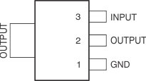
GUID-56C49ACA-2E1C-4029-BCA9-08E9398D377C-low.gif Figure 5-1 DCY Package,4 Pins (SOT-223) (Top View)
Table 5-1 Pin Functions
PIN I/O DESCRIPTION
NAME NO.
IN 3 I Input pin. See the Section 8.2.2.1 section for more details.
OUT 2, Tab O Regulated output voltage pin. See the Section 8.2.2.1 section for more details.
GND 1 Ground pin.