TIDT345 September 2023
2.3 Thermal Images
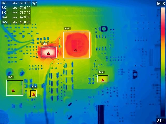
Figure 3-29 shows a thermal image of the top view of the board. Ambient temperature is 22.5°C. The board is open frame with no active air flow. Input is 48 V and output is loaded with 20 V and 3 A at VBUS for 30 minutes.

Bx1 = L1 – 20-V buck inductor
Bx2 = U1 – 20-V buck converter
Bx3 = U2 – 3.3-V buck converter
Bx4 = U4 – PD controller
Bx5 = L2 – 3.3-V buck inductor
Figure 2-4 Thermal ImageBx2 = U1 – 20-V buck converter
Bx3 = U2 – 3.3-V buck converter
Bx4 = U4 – PD controller
Bx5 = L2 – 3.3-V buck inductor