TIDT300 August 2022
3.1 Switching
Switching behavior is shown in the following figures.
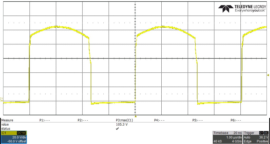
 Figure 3-1 Voltage Drain-to-Source, Q10, 57-V Input,
2.1-A Load, 20 V/div, 1 µs/div,
Figure 3-1 Voltage Drain-to-Source, Q10, 57-V Input,
2.1-A Load, 20 V/div, 1 µs/div,Measured 105.3 Vpeak
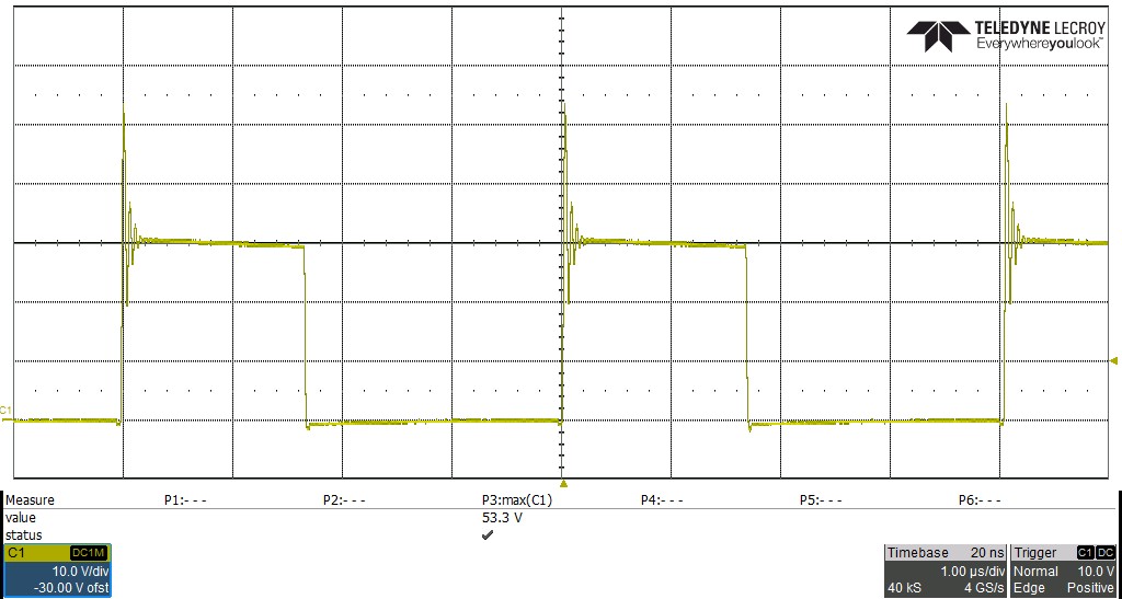
 Figure 3-2 Voltage Drain-to-Source, Q6, 57-V Input, 2.1-A
Load, 10 V/div, 1 µs/div, Measured 53.3 Vpeak
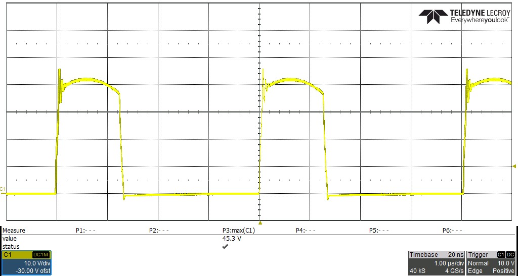
 Figure 3-3 Voltage Drain-to-Source, Q8, 37-V Input, 2.1-A
Load, 10 V/div, 1 µs/div, Measured 45.3 Vpeak