SSZTCQ9 May 2015 TPS51116 , TPS53513 , TPS53515 , TPS53915
Power system design engineers today are facing the increasing challenge of completing designs in shorter periods of time, while ensuring they’re stable over the operating environment with minimal compensation circuitry and effort. Loop compensation takes time and adds additional compensation network components increasing cost and reducing reliability. D-CAP solves this by requiring no loop compensation.
 Figure 1 D-CAP Control Mode
Advanced D-CAPTM control architecture was first invented by TI in 2004 as a form of current mode control. The term “D-CAP” means the current information is ‘Directly sensed across the output CAPacitors.’ TI’s first D-CAP controller, the TPS51116, was realized by combining a controller with a constant on-time modulator. Today, TI has a family of products featuring various modulators and next-generation forms of the original D-CAP control (Figure 1).
The three forms of D-CAP control architecture are:
D-CAP mode (with external ripple injection)
-
Features either constant on-time or a fixed frequency modulator.
-
Uses ESR at the output bulk cap to stabilize the loop.
-
DCAP with external RCC can operate all MLCC output capacitors.
D-CAP2 mode
-
An output ceramic capacitor is supported with internal phase compensation.
-
An internal inductor ripple current “emulator” circuit is used to generate a sufficient ramp for D-CAP2 control to compare the output voltage vs. the reference voltage to determine whether to turn the PWM on or not.
D-CAP3 mode
-
Supports the output ceramic capacitor with internal phase compensation.
-
The duty cycle-based adaptive ramp compensation selections are implemented by D-CAP3 to improve the transient performance and LC output filter range.
-
D-CAP3 mode improves the output voltage set-point accuracy by implementing specialized circuit(s) to remove the half time ramp magnitude. Watch “D-CAP3 control mode step-down FET converters” for more information.
Note that all forms of the D-CAP control architecture use adaptive on-time control. The PWM on time is adapted by sending the VIN, VOUT and IOUT (Figure 2).
 Figure 2 The PWM Comparator Keeps
Vo Constant
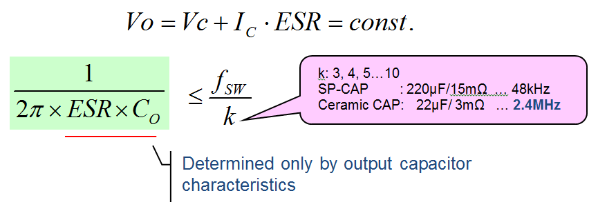 Figure 3 Loop Stability Determined
by Output Capacitors
Figure 3 Loop Stability Determined
by Output CapacitorsHow D-CAP Control Mode Works
D-CAP control mode compares a divided-down version of the feedback voltage, which comes from the output voltage ripple and contains the output voltage, to the output voltage set point, and decides whether to turn the PWM on or not. When VBF becomes lower then VREF (the output voltage set-point), the next ON period is initiated. The ON period continues for a predetermined period, and the output voltage is offset by half the output voltage ripple so the feedback design needs to be implemented accordingly (Figure 3).
D-CAP control is basically a non-linear control mode that requires no phase compensation. It delivers faster load transient response vs. voltage and current mode control for the same load transients. This results in fewer output capacitors, higher power density, lower BOM cost and higher reliability.
Seen in Figure 4 below, D-CAP control has much faster load transient response vs. voltage mode during the same load transient conditions.
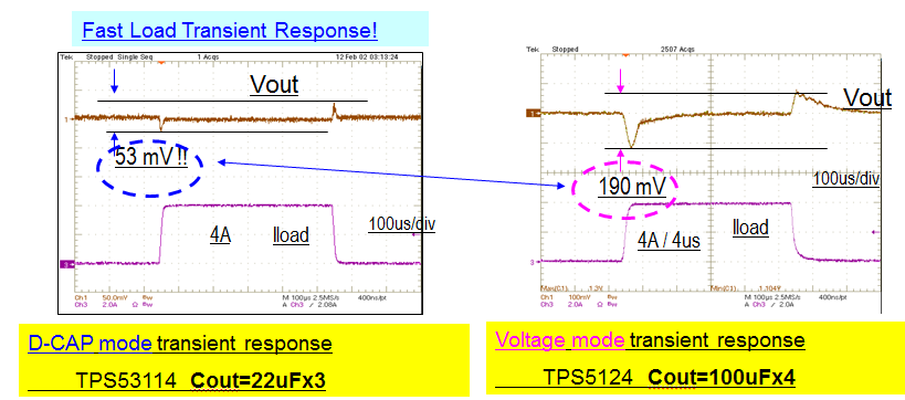 Figure 4 D-CAP Control vs. Voltage Mode
The transient response of D-CAP is fast because the ESR of the output caps provides immediate feedback of any load change. The D-CAP PWM comparator responds with an array of ON pulse in a couple of 10ns.
The ON pulse frequency increases to a very high value, and the inductor current rises to match the output current in a very short time, thus reducing the need for output capacitors (Figure 5).
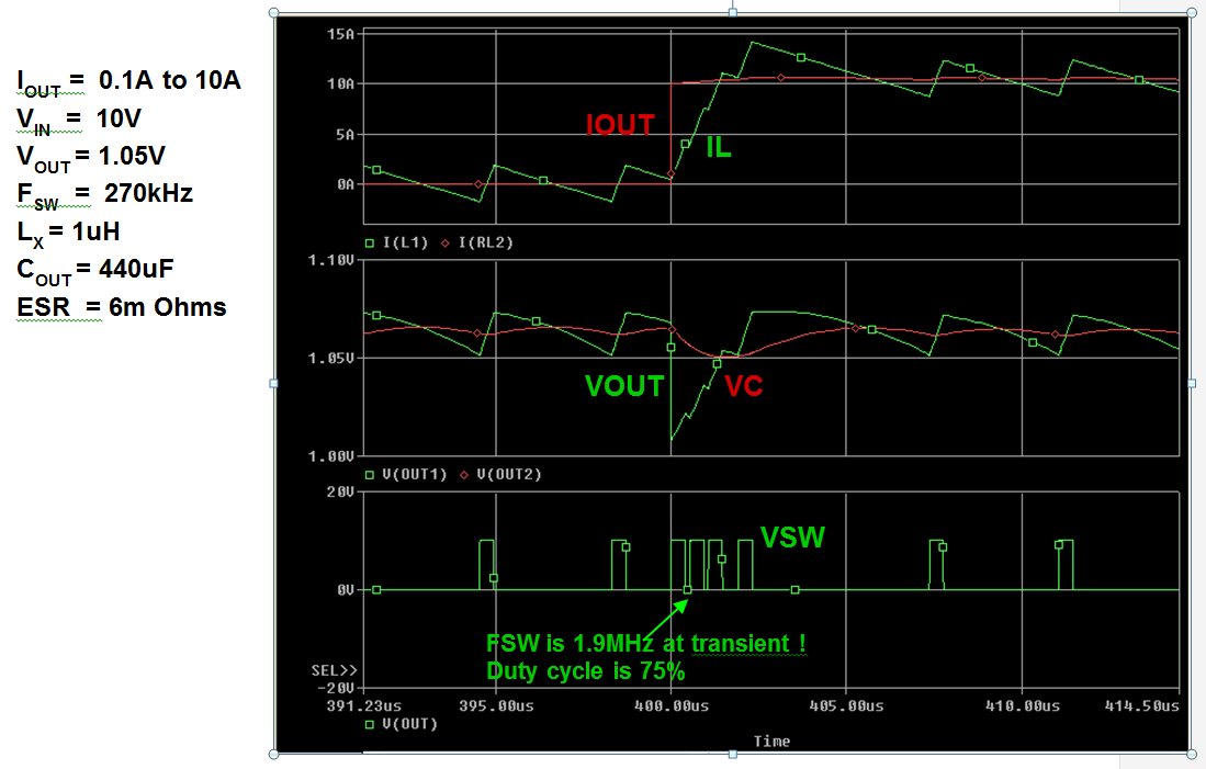 Figure 5 D-CAP Control Loop PWM Response to Load Current Changes
Voltage mode control uses an error amplifier which has bandwidth limitations. It provides the voltage and reference to the error amp but is slow in responding to a change in output voltage.
Additionally, although there is no clock in D-CAP mode DC/DC converters and controllers, the switching frequency tolerance is tight and extremely stable over the operating range (Figure 6).
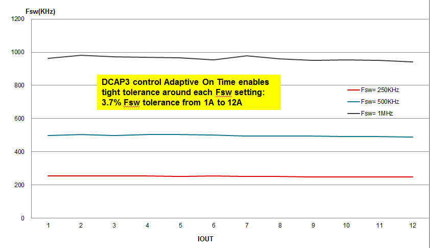 Figure 6 DCAP-3 Switching Frequency vs.
Output Current
Figure 6 DCAP-3 Switching Frequency vs.
Output CurrentD-CAP3, the most recent version, offers significant load regulation advantages vs. previous modes. It adds a special circuit to eliminate the internal ripple (ramp) DC offset when using MLCC output caps. This tightens the load regulation significantly (Figure 7). TI’s SWIFT™ TPS53513, TPS 53515 and TPS53915 converters feature D-CAP3 control Mode.
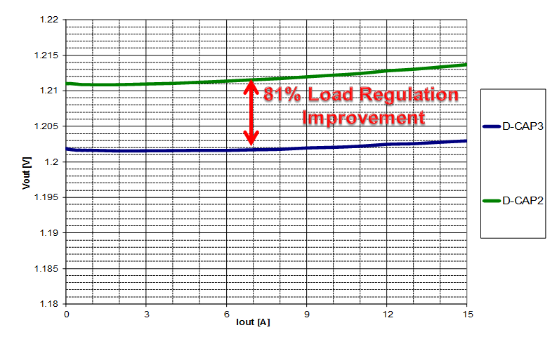 Figure 7 Load Regulation Comparison:
D-CAP2 vs. D-CAP3, 12Vin, 1.2Vout/500KHz
Figure 7 Load Regulation Comparison:
D-CAP2 vs. D-CAP3, 12Vin, 1.2Vout/500KHzAdditionally, the internal ripple (ramp) in D-CAP3 is adaptively adjusted based on the output voltage, duty ratio, output filter (LC) selection, and switching frequency to improve performance and ease of use.
With a single Rmode resistor selecting the RC (Ramp) time constant, D-CAP3 control enables optimal time and frequency domain performance as can be seen in Figure 8 below:
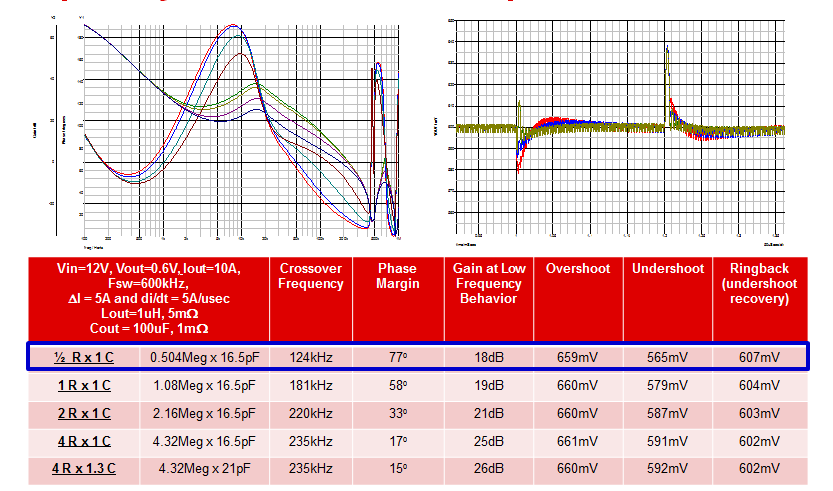 Figure 8 D-CAP3 RC (Internal RC Ramp)
Tuning for Vout=0.6V: Optimized Frequency and Time Domain Performance
Figure 8 D-CAP3 RC (Internal RC Ramp)
Tuning for Vout=0.6V: Optimized Frequency and Time Domain PerformanceReduce cost and ensure reliability in your next design with TI's products featuring D-CAP control mode. Watch “D-CAP3 control mode step-down FET converters” for more information.