SSZTCB7 august 2015 LM5160
My colleagues have written extensively about the Fly-Buck topology, but the details of the Fly-Buck’s soft/quiet switching characteristic haven’t been shared, which helps achieve higher efficiency, lower electromagnetic interference (EMI) and a smaller solution size in isolated DC/DC bias applications.
Why Flyback/buck Switching Is Noisy
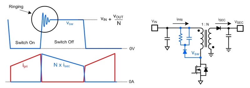
In a flyback topology, the DC voltage stress across the switch is VIN + VOUT/N. On top of this DC voltage stress, high-frequency ringing caused by the transformer leakage inductance adds more stress at the moment the switch turns off; (Figure 1[a]). A resistor-capacitor-diode (RCD) snubber is usually required on the primary side to clamp and dampen ringing at the switching node (Figure 1[b]).
 Figure 1 Flyback Topology: Simplified
Waveforms (a) and a Typical Flyback Circuit (b)
Figure 1 Flyback Topology: Simplified
Waveforms (a) and a Typical Flyback Circuit (b)It is also very common to minimize the high-frequency ringing at the switching node when designing a buck converter by using an RC snubber in parallel with the low-side switch, as shown in Figure 2(a). In a buck topology, the ringing happens at the moment when the high-side switch turns on, as shown in Figure 2(b). The printed circuit board (PCB) trace inductance and reverse-recovery characteristic of the low-side body diode both affect the amount of ringing.
 Figure 2 Buck Topology: a Typical
Synchronous Buck Circuit (a) and Simplified Waveforms (b)
Figure 2 Buck Topology: a Typical
Synchronous Buck Circuit (a) and Simplified Waveforms (b)Soft/quiet Fly-Buck Switching
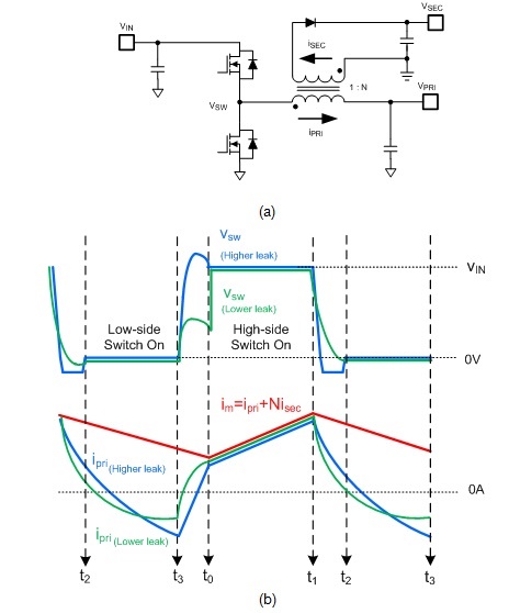
In a Fly-Buck topology, the low-side switch turns on softly because the low-side body diode conducts before the switch turns on. The energy stored in the transformer leakage inductance always has a path to flow out. The high-side switch switches quietly because the low-side body diode is reverse-biased before the high-side switch turns on. Because the low-side body diode is reverse-biased, there is no reverse-recovery current flow when the high-side switch turns on.
The DC voltage stress across the switch is VIN; see Figure 3(b). Because the Fly-Buck switching is soft/quiet, just a small margin is required on top of VIN. Figure 3 shows a typical Fly-Buck circuit and switching waveforms. In Figure 3, im is the magnetizing current, which is the combination of the primary current and secondary current reflected to the primary side.
 Figure 3 Typical Fly-Buck Circuit (a)
and Switching Waveforms (b)
Figure 3 Typical Fly-Buck Circuit (a)
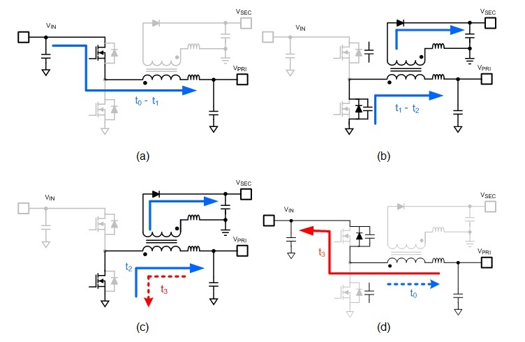
and Switching Waveforms (b)Figure 4 shows the equivalent circuits of four switching modes. The four modes are:
- MODE0: t0-t1 (energy store). The converter stores energy in the transformer when the high-side switch turns on. The primary-side current rises linearly during this period, similar to how the inductor current rises linearly in a buck.
- MODE1: t1-t2 (high-side off to low-side on dead time). When the high-side switch turns off, the primary-side current keeps flowing through the low-side body diode after fully discharging/charging the low- and high-side parasitic capacitors. The secondary-side current starts flowing since the secondary-side diode is forward-biased. The switch-node voltage becomes almost zero before t2, which allows the low-side switch to turn on softly.
- MODE2: t2-t3 (energy transfer). In this period, the low-side switch turns on and the converter transfers the stored energy to the secondary side, similar to how the flyback transfers energy to the secondary side when its low-side switch turns off. Assuming no/light load at the primary-side output, the primary-side current flows in a positive direction initially, but changes its direction to negative at the end of this period.
- MODE3: t3-t0 (low-side off to high-side on dead time). The primary-side current flows in a negative direction in this period. This current discharges/charges the high- and low-side parasitic capacitors and reverse-biases the low-side body diode. Since the low-side body diode is reverse-biased before the high-side switch turns on, the high-side switch can turn on quietly at t0, without any excessive high-frequency ringing caused by the reverse-recovery effect. The secondary-side current stops flowing in this period since the secondary-side diode is reverse-biased.
 Figure 4 Equivalent Circuit of Each
Mode and Current Flows: MODE0, T0-T1 (a); MODE1,
T1-T2 (Dead Time) (b); MODE2,
T2-T3 (c); and MODE3, T3-T0
(Dead Time) (d)
Figure 4 Equivalent Circuit of Each
Mode and Current Flows: MODE0, T0-T1 (a); MODE1,
T1-T2 (Dead Time) (b); MODE2,
T2-T3 (c); and MODE3, T3-T0
(Dead Time) (d)Conclusion
The Fly-Buck converter switches more quietly than the flyback or the buck. This quiet switching characteristic can bring some benefits beyond the Fly-Buck’s simplicity and good cross-regulation performance, including lower EMI; smaller board size, since the snubber circuit at the primary switch node is no longer necessary; and higher efficiency, by saving snubber loss on the primary side.
Additional Resources
- Download the application report, “Designing an Isolated Buck (Fly-Buck) Converter.”
- Check out the product page for the LM5160.
- Watch Robert Kollman’s video, “Power Tip 34: Design a simple, isolated bias supply.”
- Use WEBENCH Power Designer to create LM5160 Buck and Fly-Buck designs, run electrical and thermal simulations and export your customized schematic and board to popular CAD formats.
- Simulate LM5160 designs using standalone Spice Models.