SSZTBP8 January 2016 FDC2214
Capacitive sensing is an effective technique for applications ranging from proximity detection and gesture recognition to liquid level sensing. Depending on the application, there will be different system requirements regarding sensitivity, responsiveness and power. Power consumption is a key parameter for many applications, including wearables, consumer electronics and some automotive applications. So how do you reduce the power consumption of your system? In this post, I’ll describe techniques to reduce power consumption for capacitive-to-digital converters. I conducted various experiments to verify the effectiveness of these power-reducing techniques.
Duty-cycling
Capacitive sensing is currently using different circuit architectures, as I explained in my previous capacitive sensing architecture comparison blog post. In particular, the inductor-capacitor (LC) tank architecture measures the change in oscillation frequency to determine the change in capacitance. The tank oscillation frequency (fOSC) is compared to an independent reference clock (fREF) to produce an output sample that represents fOSC as a fraction of fREF. The power consumption of these types of devices is typically on the order of a few milliamps for continuous sampling modes. For low power applications, duty-cycling the device can help reduce the power consumption since the device is put into a lower-power mode and only active while it is performing a measurement conversion. This minimizes the total amount of current flowing through the device and therefore, reduces overall power consumption.
One of the main tradeoffs associated with this duty-cycling technique is responsiveness. The higher the sampling rate, the faster the system responsiveness is, but at the cost of higher average power. However, for applications that do not need an extraordinarily fast response time, a lower sampling rate can be used to achieve lower power consumption. For example, many human-machine interfaces (HMI) only need to run at sampling rates of 40 SPS or lower. The total conversion time of a measurement for a given sampling rate can also affect power consumption depending on the resolution requirements. This concept corresponds to the duty cycle of the device at a particular sampling rate.
Clock-gating
A second important technique to reduce power consumption in these capacitive sensing devices is gating of the external reference clock. Simply put, the reference clock is also turned off whenever the device is put into a low power mode. This not only reduces the power consumed by the external clock, but also significantly reduces the leakage current from the device pins.
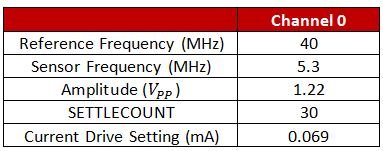
Test Setup
I tested these techniques using the TI Designs Noise-immune Capacitive Proximity Sensor System Reference Design, which uses a TI capacitive-sensing IC, the FDC2214. With only one channel (channel 0, proximity sensor) enabled, I measured the current flowing through the FDC2214 using a digital multi-meter. Figure 1 shows the test setup and the testing conditions are given in Table 1.
 Figure 1 Test Setup
|
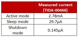
Measurements with Gated Clock
The TIDA-00466 was programmed so that the FDC2214 was only operating in one of three states: active, sleep, and shutdown. For each state, the current consumption of the device was measured and given in Table 2.
|
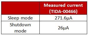
These supply current values are taken with a gated external reference clock. If the clock is not off while the FDC2214 is in sleep or shutdown mode, the power consumption in these modes will significantly increase as seen in Table 3. The clocking transitions result in an increase of the device input pin leakage currents, which is negligible when compared to the normal mode current, but is significant when added onto the lower power mode currents.
|
Measurements with Duty-cycling
Figure 2 shows an approximately linear relationship between current consumption and RCOUNT, as expected. Since RCOUNT is directly related to sensor conversion time, a lower RCOUNT results in a shorter conversion time and allows the device to spend less time actively running and more time in sleep mode (per sampling period). For a given sampling rate, a lower RCOUNT consumes less current, while a higher RCOUNT consumes more current. Another way to understand the relationship is that if RCOUNT is kept constant but the sampling rate is varied, the FDC2214 sampling at a higher rate consumes more power than a FDC2214 sampling at a lower rate.
 Figure 2 Current Consumption for Varying RCOUNT Values at Specified Sampling Rates
Summary
Duty-cycling and clock-gating are effective techniques to minimize power consumption. To ensure minimal current flow through the device, turn off the external oscillator used as the reference clock while the device is in its lower-power mode. The resulting current values for varying RCOUNT values at different sampling rates follow expected trends. Also, the FDC211x/FDC221x Current Consumption Estimator provided by TI can be used as a reference tool for estimating a worst-case power consumption scenario.
Additional Resources
- Find out more about TI’s capacitive-sensing portfolio.
- Watch this capacitive-sensing overview video.
- Read other blog posts about capacitive sensing.