SSZTBM9 February 2016 UCC28720 , UCC28722
For at least the last 20 years, MOSFETs have been the switch of choice for many switched-mode power-supply designs. Because of their higher switching speed and easier drive characteristics, MOSFETs have replaced bipolar junction transistors (BJTs) in many applications and power levels. However, for some applications – such as flyback-based low-power AC/DC chargers – BJTs have some distinct advantages over MOSFETs.
Because of their different device structure, high-voltage BJTs are less costly to make than high-voltage MOSFETs. For this reason, BJTs with voltage ratings up to or over 1kV are available for a lower price than the 600V or 650V MOSFETs often found in universal-input offline-flyback converters.
The advantage is immediately obvious. Because of the BJT's higher voltage rating, the leakage spike can be several hundred volts higher and yet still within the required switch derating. Depending on the magnitude of spike, it is often possible to remove the snubber completely without over-volting the switch.
Removing the Snubber
Advantages:
- Reduces the number of components on the bill of materials (BOM), allowing a smaller, and more cost-effective solution. Most significantly, you can remove the snubber diode, which is generally a 600V part.
- Reduces the number of components connected to the high-voltage switching node, thus reducing the area of this node. Because of the high instantaneous voltage rate-of-change over time (dv/dt) and the large voltage swing, any parasitic capacitance from this node causes significant unwanted currents. These currents can generate noise signals that can interfere with the controller or other devices on the board, or electromagnetic interference from the power supply, requiring filtering to meet harmonic emission standards.
- Increases efficiency by saving the power dissipated by the steady-state voltage across the snubber resistor (= Vreflected/Rsnubber2 ).
High-input Voltages
Another area where you can take advantage of a BJT's high voltage rating is in applications with high-voltage or three-phase inputs. A standard European 230V three-phase input will have a peak line-to-line voltage of ~565Vdc. This peak voltage is often a rating requirement for equipment connected across a single phase, in case a fault in one phase of the load causes the neutral to be pulled to one of the line voltages. While many designers achieve the switch rating for this condition by using a large, expensive and higher-RDSON MOSFET or by cascading two lower-voltage MOSFETs in series to achieve the desired rating, using a single high-voltage BJT instead reduces both system size and cost.
Design Considerations- EMI.
Designers who remove the snubber may be concerned that the unsnubbed voltage ring will increase the conducted emissions from the unit and require extra filtering.
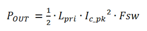
Figure 1 through 4 show the difference in conducted emissions for the same unit with the snubber fitted and removed. The waveforms show the difference in the leakage inductance spike in both cases.
As you can see, removing the snubber does not cause any measureable difference in conducted emissions at the frequency of the leakage inductance ring (~15MHz).
 Figure 1 Conducted emissions plot at
230VAC – 6.5W load, no snubber fitted
Figure 1 Conducted emissions plot at
230VAC – 6.5W load, no snubber fitted Figure 2 Conducted Emissions Plot at
230VAC – 6.5W Load, Snubber Fitted per the Waveforms in Figure
3
Figure 2 Conducted Emissions Plot at
230VAC – 6.5W Load, Snubber Fitted per the Waveforms in Figure
3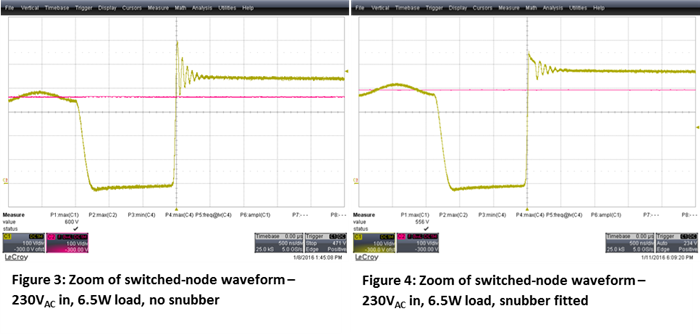
Design Considerations- Drive Circuit.
A combination of the base drive current, the current gain of the transistor and the magnetizing inductance of the flyback transformer dictate the peak power which a BJT flyback can supplype. Together, these parameters must be able to support the primary peak current required to deliver the desired output power at the operating frequency.
POUT for a discontinuous-mode flyback:
where
A BJT used as a switch must be driven into saturation during the on interval to minimize on-state conduction losses. In other words, you must supply the BJT with more base current than is required to generate the collector current, which will be allowed to flow by the primary inductance:
When the base voltage goes below Vth, the time that it takes for excess carriers in the base to recombine, delays the turn-off of the FET. It is desirable to minimize the duty cycle of this turn off delay and for this reason the switching frequency range on BJTs is limited, typically to about 60kHz or so.
Ideally, the base current supplied is such that the device is just passing from the saturation region to the active region at the end of the on time, reducing the number of excess carriers at turn off and reducing the turn-off delay.
 Figure 3 Device Region v Ic, Ib and
Vce
Figure 3 Device Region v Ic, Ib and
VceThe more complicated drive required by BJTs is one reason why MOSFETs have replaced them in many applications. Devices such as TI’s UCC28720 and UCC28722 have addressed this issue by dynamically adjusting the drive current with load. At lower load levels, the reduced base current ensures that there is not a large amount of excess charge in the base region upon turn-off.
These devices also feature a 1W pull resistance on the drive pin to short the base-emitter junction during the off time so that the BJT can sustain the rated collector-to-emitter (VCES) voltage. To sustain the VCES rating, it is important to short the base node to ground through a low-impedance connection during the off time, and that the collector current has stopped flowing before the collector voltage rises above Vceo to avoid second breakdown.
The UCC28720 and UCC28722 simplify the drive for system designers and make power BJTs drop-in solutions for low-power flybacks, reducing component count and system cost.
Additional Resources:
Download the TI Designs Snubberless, Non-Isolated AC/DC Flyback Converter Reference Design with Simplified Transformer
Design using UCC2872x parts.