SSZTBJ4 march 2023 LM5017 , LM5160
Isolated power supplies are often required in many industrial and enterprise applications. Designing such power supplies requires the use of an optocoupler for feedback control, which adds another level of complexity. TI’s LM5017/8/9 and LM5160 constant on-time (COT) synchronous buck regulator family has specific features that enables its use in a fly-buck topology that can eliminates the need of an optocoupler and greatly reduces the design complexity, the cost of the bill-of-materials (BOM), and the cost of the printed circuit board (PCB).
A traditional fly-buck uses a diode to rectify the isolated output; however, the output regulation of this approach degrades as current increases, resulting in poor efficiency and thermal performance. One method to maximize current delivery while maintaining acceptable efficiency and regulation is to use a synchronous rectifier. The TI Designs 15W Isolated Self-Driven Synchronous Inverting Fly-Buckboost Using LM5160 Regulator Reference Design is an example of using the LM5160 regulator as a fly-buck to generate a 5V output capable of supplying 3A of continuous current. This design uses a self-driven winding to drive the gate of a synchronous rectifier. Figure 1-1 shows the primary side configured as an inverting buck-boost configuration, the reason why is described in more detail later.
 Figure 1-1 Self-Driven Block
Diagram
Figure 1-1 Self-Driven Block
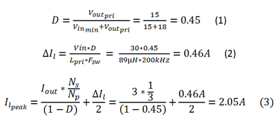
DiagramLoad regulation can be impacted if the 1-D period is less than 50% as a result of energy being transferred to the secondary side during this period. As the 1-D period decreases, the peak current on the primary during the 1-D period greatly increases for a given load. As a result, the peak currents get larger and the load regulation is greatly impacted, as more of the voltage on the primary is distributed across the magnetizing inductance and leakage inductance. Therefore when designing a fly-buck, it is recommended the 1-D period is greater than 50%. In addition, the LM5160 peak current limit can be as low as 2,125A (2.5A typical), in order to meet the 3A requirement without going into current limit the specific turns ratio was selected. The design uses a Versa-Pac transformer with a 3-to-1 step-down ratio. Equation 1 and 2 show the peak inductor current at Vinmin:
In order to drive the synchronous MOSFET during the off time, a nine-turn winding is installed on the transformer which produces a 2-to-1 turns ratio. Equations 4 to 7 show the Vgs voltage of the synchronous FET during duty on and duty off at Vinmax:
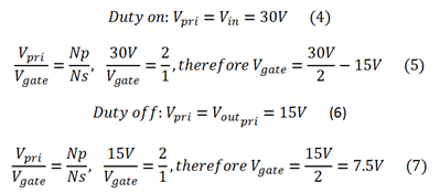
 Figure 1-2 Vgs At Maximum
Vin
Figure 1-2 Vgs At Maximum
VinTransformer’s leakage inductance, DC resistance (DCR) and rectifier’s forward-voltage drop are the contributing factors for output regulation for fly-buck output regulation, Figure 1-3 shows that this design is able to achieve ±5% regulation across entire Vin and load range using the synchronous rectifier.
 Figure 1-3 Load Regulation across Vin
Range
Figure 1-3 Load Regulation across Vin
RangeAt no load, the secondary output voltage may peak charge due to voltage spikes at the secondary if a diode rectifier is used. This synchronous approach also eliminates the need of a preload resistor or Zener clamp for regulation at no load.
You can further improve regulation and efficiency by making a dedicated transformer with lower leakage inductance and DCR compared with the Versa-Pac. Also, a dedicated synchronous winding that is closely coupled with the primary winding will reduce the switching spikes and avoid exceeding the maximum voltage rating between gate and source of the synchronous MOSFET.
Additional Resources
- Explore more power-supply topics.
- Watch Power Tips videos to help with your design challenges