SSZTAW7 september 2016 UCC28019A , UCC28051 , UCC28063 , UCC28070 , UCC28180
Power factor correction (PFC) forces the input current to follow the input voltage (VIN) so that any electrical load appears like a resistor. This action requires sensing the input voltage and modulating a current reference based on that sensing. The current loop will force the input current to follow the reference. This is called average current-mode control, as shown in Figure 1.
 Figure 1 PFC Average Current-mode
Control
Figure 1 PFC Average Current-mode
ControlYou can find lots of commercial PFC controllers with low total harmonic distortion (THD) using this average current control algorithm in the market. However, these PFC controllers need a dedicated pin to sense VIN and a precision analog multiplier for current-reference modulation.
Another PFC control algorithm that does not need VIN sensing but can still provide average current-mode control has become very popular recently. TI’s UCC28180 belongs to this family. Because it lacks a VIN sense pin and the precision analog multiplier, it comes in a smaller package, enabling lower system cost, and is very easy to use.
But when we introduce the UCC28180 to designers, many times their first response is, “What? Without VIN sensing? How does that work?” In this post, I will try to answer this question.
Figure 2 shows the control algorithm used in the UCC28180. A low-bandwidth voltage loop regulates the output voltage. The input current is measured as VIin and compared with a saw-wave Vramp. The amplitude of Vramp is proportional to the voltage-loop output. Because PFC uses the boost topology, the input-voltage information is already there, but hidden. The control algorithm shown in Figure 2 employs the hidden information.
 Figure 2 PFC without VIN
Sensing
Figure 2 PFC without VIN
SensingThe PWM output signal always starts low at the beginning of the switching cycle, triggered by the internal clock, as shown in Figure 3. The PWM output stays low until Vramp rises linearly to intersect the VIin voltage. The Vramp/VIin intersection determines switch turning off time tOFF.
 Figure 3 PWM Generation
From Figure 3:
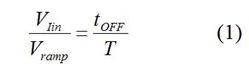
Here T is the switching period. For boost converter operating in continuous conduction mode (CCM):
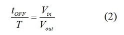
Combining Equations 1 and 2 gives you Equation 3:
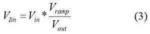
The voltage output, VOUT, is a constant in steady state. Since the PFC voltage loop is very slow, Vramp is also a constant in steady state. Thus, the input current is solely proportional to VIN. If VIN is sinusoidal, the input current must be sinusoidal, achieving good PFC. It looks like magic, doesn’t it?
Learn more about TI’s PFC solutions.
Additional resources:
- Get started designing with the UCC28180:
- Get to know the UCC28051, UCC28063, UCC28019A and UCC28070
- Read more of Bosheng's blogs
on PFC:
- It is not just a PFC controller, it is also a power meter
- How to reduce PFC harmonics and improve THD using harmonic injection: Part 1, Part 2
- How To: Improve power factor and THD using DFF control