SSZTAD8 march 2017 LM34936 , LM5175 , LM5176 , LM5176-Q1
In my last blog, I provided tips for optimizing hot loops in a buck-boost converter. I decided to add this tip as a separate topic after finding it in almost all of the layouts I reviewed late last year. The most frequently encountered issue in layout is the incorrect routing of differential sense signals from the sense resistor to TI’s LM5175 integrated circuit (IC) pins (the CS-CSG pair). An example of sense connection is shown in Figure 1.
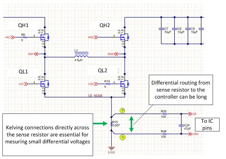 Figure 1 An LM5175 Schematic Showing
Differential Sense Connection from Power Stage to the Controller Pins.
Figure 1 An LM5175 Schematic Showing
Differential Sense Connection from Power Stage to the Controller Pins.In some cases, designers make this error because one of the sense nodes (the lower side of the sense resistor, marked as node “N” in the yellow circle) is electrically same as the circuit ground (GND). Thus, the need to differentially route the CS-CSG pair – which carries a small signal (tens of millivolts) – is not clear to the layout engineer. Figure 2 shows this common error.
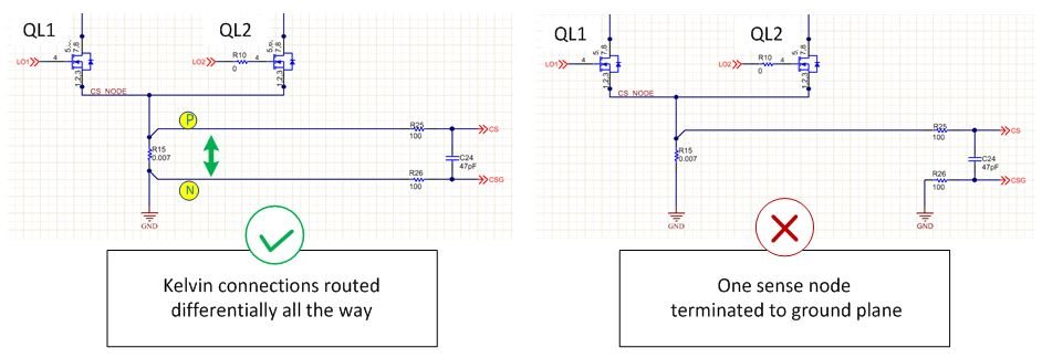 Figure 2 (a) Correct Differential
Current Sense Routing and (b) a Common Mistake When Routing Differential Sense
Signals.
Figure 2 (a) Correct Differential
Current Sense Routing and (b) a Common Mistake When Routing Differential Sense
Signals.In other cases, the designer does recognize the need to differentially route the current-sense signals. But during the finishing of the board, the negative trace is connected to a plane or a copper pour, as the layout tool treats the nets as a ground (GND) net. This unintended connection can happen anywhere along the trace, as shown in Figure 3. In the next paragraphs, I will describe some common practices to avoid this.
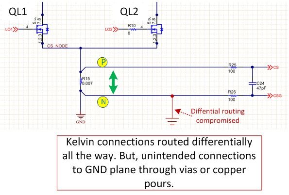 Figure 3 An Example of Unintentional
Connection of Differential Sense Signal with Power Ground Plane.
Figure 3 An Example of Unintentional
Connection of Differential Sense Signal with Power Ground Plane.Net Ties
A net tie allows an artificial separation of net names in the schematic (Figure 4). This allows the layout tool to treat N1 and N2 as separate nodes and protects the bulk of the differential trace (N2) from accidental connections to the ground plane or pours. The downside is that the N1 section is technically a GND net, and therefore still needs to be separated from the GND plane or copper pours (Figure 4).
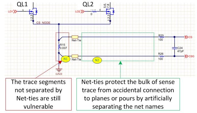 Figure 4 An Example of Using Net-Tie to
Prevent Unintentional Connection of Sense Signals to Copper Planes or
Pours.
Figure 4 An Example of Using Net-Tie to
Prevent Unintentional Connection of Sense Signals to Copper Planes or
Pours.Polygon Cutouts or Keep Outs
Many layout tools provide a feature called polygon cutouts or polygon keep outs. Polygon keep outs create a boundary that keeps polygons or copper pours from entering. A polygon keep-out layer must follow the sense trace from beginning to end. You must take additional care when the sense trace changes layer though vias. In such cases, you must use polygon keep outs on all layers around the via. Figure 5 shows an example.
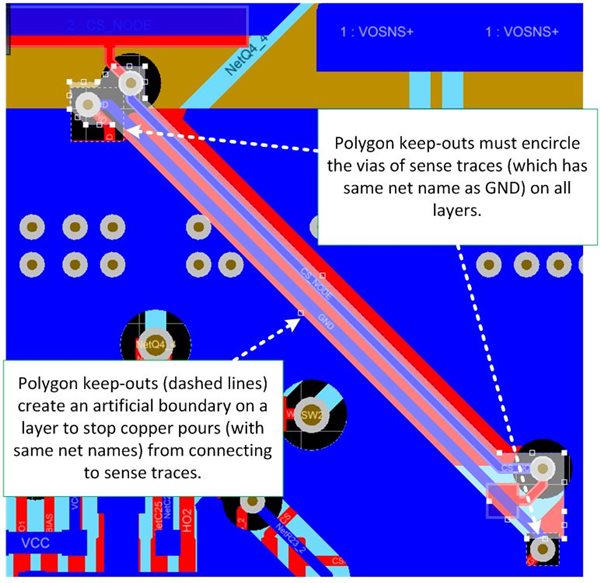 Figure 5 Correct Use of Polygon
Cut-outs to Separate Sense Traces from Power Planes.
Figure 5 Correct Use of Polygon
Cut-outs to Separate Sense Traces from Power Planes.The incorrect routing of sense traces can spoil an otherwise good design. Recognizing the sense traces – particularly those that share the net names with a copper area, plane or pour – is essential. These traces must be isolated using net ties or polygon keep outs during printed circuit board (PCB) design to prevent an inadvertent connection to the copper planes.
Additional resources:
- Read the previous installments of this series: "Four-switch buck-boost layout tip No. 1: identifying the critical parts for layout" and "Four-switch buck-boost layout tip No. 2: optimizing hot loops in the power stage"
- High Density PCB Layout of DC/DC Converters, Part 1
- High Density PCB Layout of DC/DC Converters, Part 2
- DC/DC Converter PCB Layout - Part 3
- DC/DC Converter PCB Layout - Part 2
- DC/DC Converter PCB Layout - Part 1