SSZTA27 June 2017 LM25145 , LM5145
At the epicenter of most power converter implementations is the inevitable trade-off of efficiency and power density. However, new applications are coming to fruition that have unique power solution requirements. Many designers are choosing to capitalize on demonstrated and verified power solutions using buck controllers that combine performance and flexibility.
With industrial and communications applications in mind, two key performance attributes are:
- A wide input voltage (VIN) range for large step-down ratios, high reliability and low solution cost.
- Flexible, easy-to-use designs with design tool support for faster design-in and time to market.
Wide vIN Range
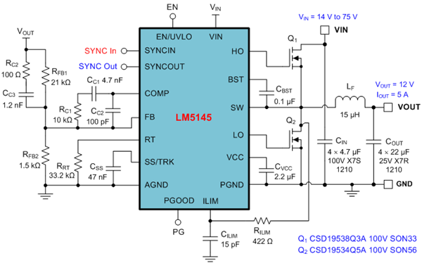
A controller with a wide VIN range and low minimum on-time (also known as TON-min) facilitates large input-to-output voltage differentials and direct step-down conversion from a nominal 24-V, 28-V, 48-V or 60-V bus to a low-voltage output for reduced system complexity and low solution cost. As an example, take a look at the synchronous buck controller circuit shown in Figure 1.
 Figure 1 Schematic of a Wide
vIN Synchronous Buck-Controller Solution with a 12-V, 5-A Output
at 300 kHz
Figure 1 Schematic of a Wide
vIN Synchronous Buck-Controller Solution with a 12-V, 5-A Output
at 300 kHzDesigned to regulate from a high VIN source or an input rail subject to high voltage transients, a wide VIN controller minimizes the need for external surge suppression components to reduce both solution size and cost without sacrificing reliability. Such an outsized voltage rating delivers the higher operating margins and transient immunity performance critical in applications that require an extended product life cycle, such as communications, industrial, medical and motor-drive systems.
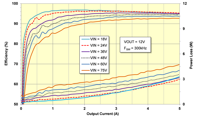
Figure 2 shows the efficiency plot for the regulator in Figure 1. For this measurement, the LM5145’s VCC is powered from VOUT to reduce bias power dissipation and increase light-load efficiency. Moreover, the integrated 7.5-V gate drivers reduce MOSFET dead time and body diode reverse-recovery losses to raise efficiency at heavy loads.
 Figure 2 Synchronous Buck-Regulator
Efficiency with Output-Derived Bias Power and Discontinuous Conduction Mode
(DCM) Enabled at Light Loads
Figure 2 Synchronous Buck-Regulator
Efficiency with Output-Derived Bias Power and Discontinuous Conduction Mode
(DCM) Enabled at Light LoadsEase of Use
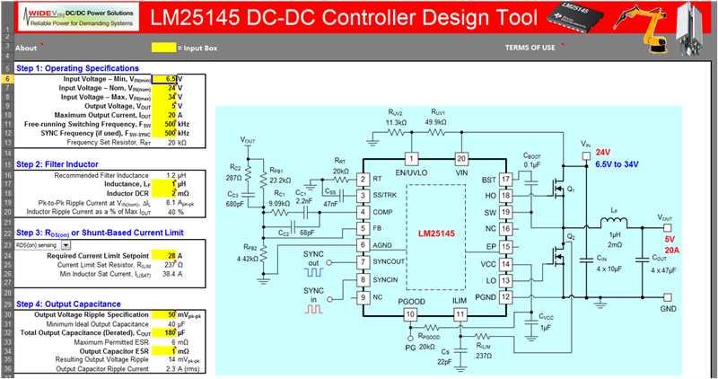
To bridge the divide between ease of use and high-performance power-conversion integrated circuits (ICs), TI offers a range of power design tools, including WEBENCH®, PSPICE simulation models and the TI Designs reference design library. And given the component interdependencies and trade-offs inherent to high-performance solutions, an IC-specific quick-start calculator is another convenient tool to expedite and streamline the design process. For example, the screen capture of the Excel-based controller design tool in Figure 3 illustrates a step-by-step design flow for an LM25145 500-kHz buck-regulator solution with an output rated for 5 V and 20 A. The LM25145 quick-start calculator is available as a free download.
 Figure 3 Buck-Controller Quick-Start
Calculator – the Schematic is Auto-Populated Based on Entered and Calculated
Component Values
Figure 3 Buck-Controller Quick-Start
Calculator – the Schematic is Auto-Populated Based on Entered and Calculated
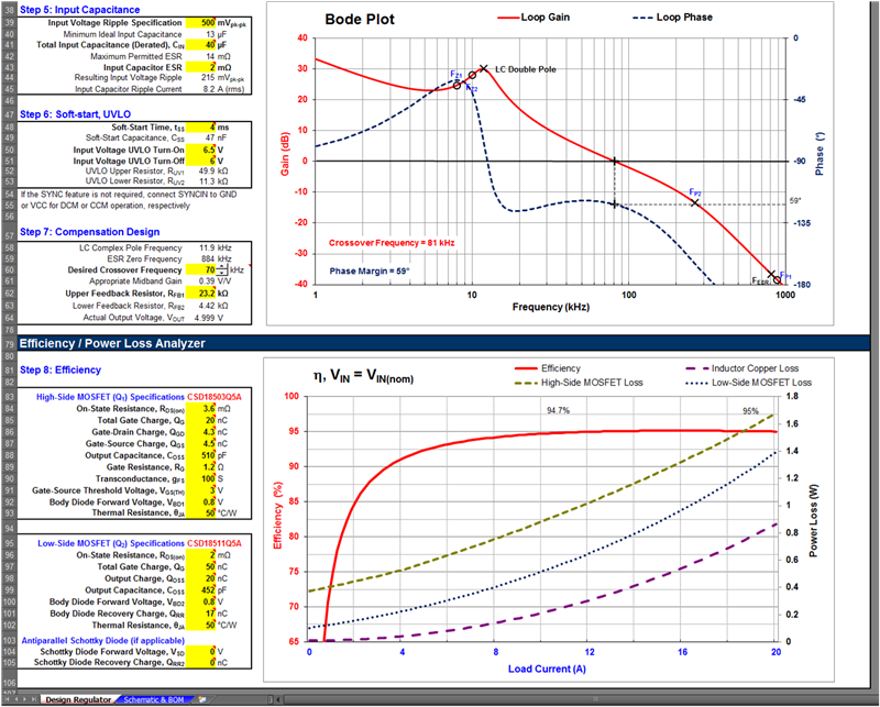
Component ValuesStep 1 in Figure 3 enables the user to enter specifications for input voltage range, output voltage, full load current and switching frequency. Step 2 considers buck inductor selection, and Step 3 considers overcurrent protection. The subsequent design steps shown in Figure 4 assist with input and output capacitance, soft start, undervoltage lockout, and loop compensation component selection.
 Figure 4 LM25145 Quick-Start Calculator
with Bode Plot, Efficiency and Component Power Loss Analyses
Figure 4 LM25145 Quick-Start Calculator
with Bode Plot, Efficiency and Component Power Loss AnalysesWith calculations based on the parameters entered for the power MOSFETs and passive components, Figure 4 also shows the predicted Bode plot and regulator efficiency sweep. Application example No. 1 from the LM25145 data sheet presents more details related to this particular design, including recommended power stage components, operating waveforms and printed circuit board (PCB) layout guidelines for high density and low electromagnetic interference (EMI).
Summary
Amid a continual focus on high conversion efficiency and low overall bill-of-materials cost, a wide VIN synchronous buck controller dovetails seamlessly into a variety of power stage circuits for industrial control and communications infrastructure applications. The footprint and feature-set compatibility of the LM5145 and LM25145 family, aided by a broad set of regulator design tools, entwine performance and flexibility in designs with output currents ranging from 5 A to 25 A.
Additional Resources
- Download the LM5145 quick-start calculator.
- Order the evaluation module for the LM5145 synchronous buck controller.
- Read the application note, Reduce buck-converter EMI and voltage stress by minimizing inductive parasitics
- Review these white papers: