SSZT959 september 2017 LM25017 , LM5160 , TPS55010

Traditionally, designers have used flyback converters and push-pull drivers with transformers for generating an isolated power supply. The Fly-Buck™ converter (or isolated buck converter) has gained popularity as a low-power isolated bias solution because of its simplicity, ease of implementation and low bill of materials (BOM) cost for uninterruptable power supply (UPS) designers.
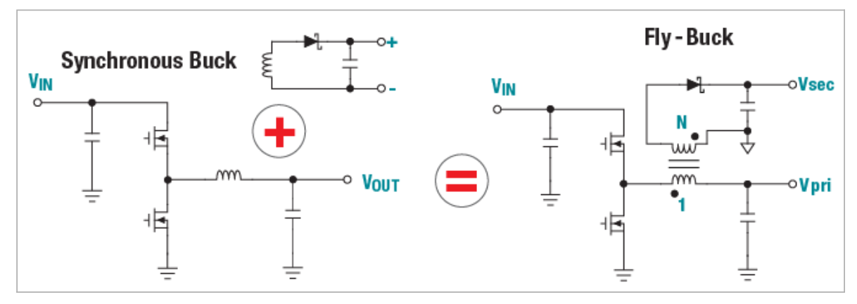
The Fly-Buck converter evolved from a synchronous buck converter by adding coupled windings to the inductor for isolated outputs as shown in Figure 1.
 Figure 1 Evolution of a Synchronous
Buck Converter to a Fly-Buck Converter
Figure 1 Evolution of a Synchronous
Buck Converter to a Fly-Buck ConverterFly-Buck converter results in a simpler solution than a flyback converter at lower power levels because of the integrated field-effect transistors (FETs) and the absence of any external feedback loop. The attractiveness of the topology has been mostly at low power levels (< 15W), where tight regulation on the secondary voltage is not required, such as in power supplies for gate drivers.
The Fly-Buck converter also offers the primary non-isolated buck output at no additional cost. Therefore, it results in a simpler design for applications that require both isolated and non-isolated outputs.
However, you cannot configure every buck converter as a Fly-Buck converter.
Choosing a Synchronous Buck Converter
In a Fly-Buck converter, the low-side switch cannot be a diode as it is in a nonsynchronous buck. In a Fly-Buck converter, the primary current flows in the reverse direction during the off time due to the reflected secondary-side current on the primary side and may become negative. The diode in a nonsynchronous buck will block this negative current, which blocks the energy delivery to the secondary. As a result, the isolated output voltage will collapse.
For some synchronous buck-converter integrated circuits (ICs), the low-side FET turns off (for example, in pulse-frequency modulation [PFM] mode) if negative inductor current is detected, thus increasing light-load efficiency. In such cases, the FET emulates the diode behavior, making such buck converters unsuitable for a Fly-Buck converter. However, in some converters you can disable the diode emulation mode so that the converter works in forced pulse-width modulation (PWM) mode. You can use such converters as a Fly-Buck converter. An example of such a converter is TI’s LM5160.
Choosing the Right Control Scheme
Not all control schemes are fit for Fly-Buck converters. Because the primary-side current in the off time is different than a normal buck, current-mode control relying on low-side FET current or valley-current sensing will not be the right choice for a Fly-Buck converter.
Choosing the Right Current-limit Scheme
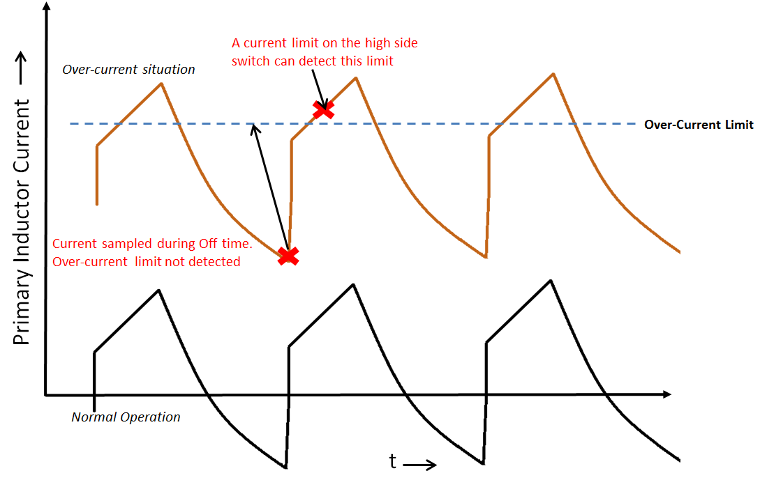
To incorporate overcurrent/short-circuit protection, a synchronous buck IC that has a current limit on the high-side switch is a good choice, since the current waveform in a Fly-Buck converter during its on time is similar to a normal buck converter. The primary current flows in the reverse during the off time due to the reflected secondary-side current on the primary side and can become negative. For ICs that have only a valley detection control circuit, where the switch current is monitored during the off state, the overcurrent situation may not be detected (see Figure 2). Such a situation may damage the IC.
You should choose the peak current limit based on the design requirements, especially considering a situation where the primary side is not loaded and the secondary side is shorted. Some ICs also have negative overcurrent protection (when the converter sinks current through its low-side FET) that detects voltage across the low-side metal-oxide semiconductor field-effect transistor (MOSFET) and allows the control circuit to turn off the low-side MOSFET if the reverse current exceeds the negative current limit. An example of such a converter is TI’s TPS55010.
The LM25017 is a good fit for a Fly-Buck converter, as it operates in continuous conduction mode (CCM) regardless of the output loading. The device has constant on-time (COT) control, which is not affected by the current waveform, current-limit protection in the high-side (buck switch) FET, and an adaptive current limit off-timer.
 Figure 2 Overcurrent/short Circuit in a
Fly-Buck Converter
Figure 2 Overcurrent/short Circuit in a
Fly-Buck ConverterReference Design for an Isolated Gate Driver Supply
The Compact, Single-Channel, Isolated SiC and IGBT Gate Driver Reference Design for UPS and Inverters employs a 1.5W Fly-Buck converter configuration for powering isolated silicon carbide (SiC) and isolated gate bipolar transistor (IGBT) gate drivers used in UPSs, DC inverters and electric vehicle charging station applications to drive the power stages. The isolated Fly-Buck converter power supply is realized using the LM25017 in a 33mm-by-23mm form factor. Additionally, this reference design provides a fully tested, robust, independent, easy-to-validate, single-channel driver solution capable of withstanding >100kV/μs common-mode transient immunity (CMTI). The reference design guide has comprehensive details of the Fly-Buck converter design and implementation.
Additional Resources:
- Learn more about TI’s Fly-Buck™ solutions for your industrial design
- Read more about Fly-Buck™ topology from TI’s e2e blogs
- Download the Compact, Single-Channel, Isolated SiC and IGBT Gate Driver Reference Design for UPS and Inverters