SSZT293 june 2020 TPS562200 , TPS562201 , TPS562208 , TPS562209 , TPS562210A , TPS562219A , TPS562231 , TPS563200 , TPS563201 , TPS563208 , TPS563209 , TPS563210A , TPS563219A , TPS563231 , TPS563240 , TPS563249 , TPS62912 , TPS62913 , TPSM82913
Your new design needs to fit twice as much into half the space and cost nothing – sound familiar? You selected the smallest point-of-load regulator and generated the tightest layout you could with the most cost-effective passive components. So far so good. But then you look at the output ripple on your critical rails and it’s not what you expected. What’s going on?
Let’s start by understanding what makes up the output ripple on a buck DC/DC regulator. It is a composite waveform. Traditionally only the three dominant elements shown in Figure 1 have been considered:
- A triangular wave generated by applying the inductor current ramp across the equivalent series resistance (ESR) of the output capacitors. A 22-µF X5R ceramic capacitor may have an ESR of only 2 mΩ. Considering an inductor peak-to-peak current ripple of 1 A, the ESR ripple is 2 mV (less if you’re using multiple parallel capacitors).
- A pseudo-sinusoidal component due to output capacitance. For the same output capacitor and ripple current as in the bullet point above, the capacitive ripple will be around 8 mV (less for multiple parallel output capacitors).
- A square component generated across the output capacitor equivalent series inductance (ESL). For a 22-µF X5R capacitor, the ESL is around 0.5 nH, which generates a ripple of about 2 mV.
 Figure 1 Typical Output Ripple
Waveforms
Figure 1 Typical Output Ripple
WaveformsHowever, what you measure has spikes on the edges and a higher square-wave content that changes polarity when you reverse the inductor shown in Figure 2:
 Figure 2 Measured Output Ripple
What has caused these undesirable components? And more importantly, what can you do about it?
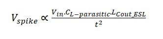
Spikes
When you selected your inductor, the self-resonant frequency (SRF) was above your regulator switching frequency, so all was good. Let’s re-look at that – the inductor has an SRF because it has a parallel parasitic capacitance. Applying the fast edge of the switching voltage to the parasitic capacitance generates a large current spike through the capacitor, which in turn generates a large voltage spike across the ESL of the output capacitor:
To reduce this spike:
- Select an inductor with a smaller parasitic capacitance. Look for the highest SRF value for the inductance and rating you need. Lower inductances tend to have lower parasitic capacitance (as do lower current ratings), so don’t over-specify the inductance or current rating.
- Reduce the output capacitance ESL. Choose the smallest capacitor package size that meets your output capacitance requirements. Using multiple smaller capacitors in parallel means the package size (and hence the ESL) of each capacitor can be smaller, while having inductors in parallel will also reduce the total ESL.
- Reduce the transient voltages (dV/dt) of the switch node (increase the value of t). Some regulators may allow direct control of the switch-node edge, but more often you may be able to place a small resistor in series with the bootstrap capacitor to slow the edge. This can impact efficiency, so the first two options are preferable.
Square Wave
Let’s say that you selected a cost-effective, unshielded inductor. The magnetic field from an unshielded (or resin-shielded inductor) can spread beyond the physical body of the component. The simulation plots in Figure 3 show the field for an unshielded open drum inductor and a fully shielded molded inductor.
") Figure 3 Magnetic Field for Unshielded Drum and Shielded Molded Inductors (Source: Courtesy of Coilcraft)
Figure 3 Magnetic Field for Unshielded Drum and Shielded Molded Inductors (Source: Courtesy of Coilcraft)- Select a shielded inductor to reduce the leakage flux that generates this coupling. If you’re using unshielded or semi-shielded inductors, selecting an inductor that is larger in the x-y dimension but has a lower profile will reduce the airgap height and hence the fringing flux.
- Reduce the output capacitance ESL as described above.
- Don’t position the output capacitors and tracking directly next to the inductor, where the field is highest. Where space is critical, consider placing the inductor on the opposite side of the board to the rest of the regulator circuit in a clamshell construction. This moves the output capacitors away from the plane of the inductor where the magnetic field is strongest.
Additional resources
- Read the Analog Design Journal article, “Select inductors for buck converters to get optimum efficiency and reliability.”
- Download the application reports, “Output Ripple Voltage for Buck Switching Regulator” and “Space Optimized, ‘Clam-Shell’ Layout for Step-Down DC/DC Converters.”