SNVAA54 October 2022 TPS563202 , TPS564242 , TPS564247 , TPS565242 , TPS565247 , TPS566242 , TPS566247
TPS56X242/7 Pin Out with Integrated BST Cap
With technology development, the end equipment trend is smaller, smarter, and more powerful. As for the power management IC, there is a strong trend towards smaller size, higher power density, and easier to use.
Now in market, SOT563 package is more and more popular in DC/DC converter. This package has advantages of small size, easy to use, and so on. Many companies release the SOT563 package parts. TI first releases the 16-V/6-A part on SOT563 package by optimizing layout to increase power density.
Figure 1-1 is TPS566242/7 pin out with SOT563 package. This pin out has a little difference with last generation part TPS563202 3-A part as Figure 1-2. Most of the pin are same. The only difference is definition of pin 4. Please see Table 1-1. The Pin 4 of TPS563202 is BST pin. TPS566242 integrates BST pin by using a special charging high side FET circuit and optimizing the high side driver circuit. TPS566242/7 high side FET still uses N-MOSFET. With optimizing the driver circuit, TPS56x242/7 has very good efficiency which can get 94% at 12-V input voltage to 5-V output voltage at 6-A loading.
| Part Number | Pin Number | Pin Name | Description |
|---|---|---|---|
| TPS566242 | 4 | AGND | Ground of internal analog circuitry. Connect AGND to the GND plane. |
| TPS563202 | 4 | BST | Supply input for the high-side NFET gate drive circuit. Connect 0.1 µF capacitor between BST and SW pin. |
The advantage of integrated BST cap not only helps customer to save one BST cap, but also makes the layout easy, improves thermal performance. And current pin out still can do the co-layout with the pin out of last generation part.
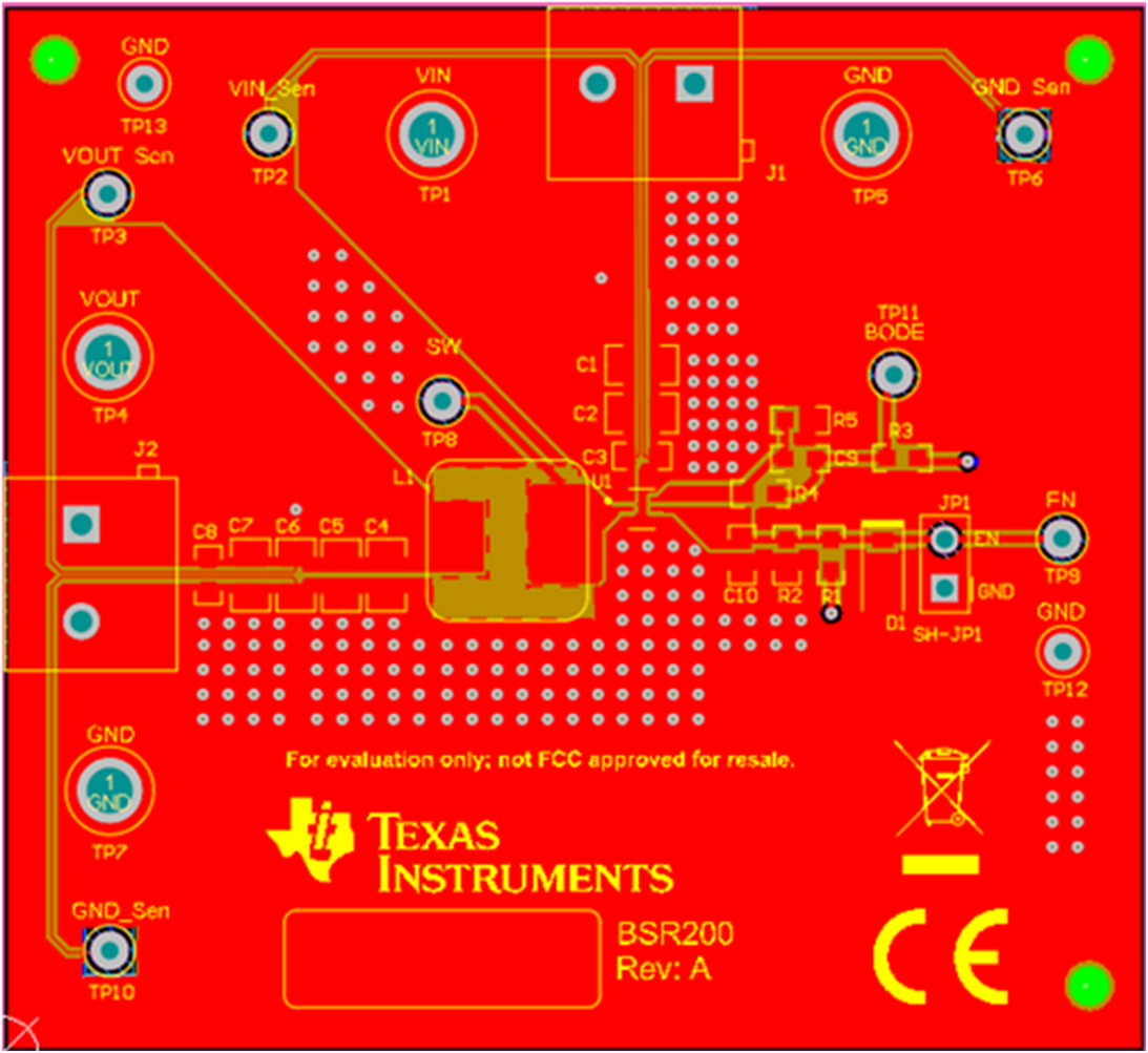
The pin out of TPS566242 is very easy to do the layout . We recommend to do the layout as Figure 1-3. GND and AGND are connected together to improve thermal performance. TPS566242 can even realize the single side PCB as Figure 1-4. Several customers prefer to use single-side PCB board to save cost. TPS563202 has a BST pin which needs a BST cap to connect to SW pin in Figure 1-5. Because the top layout limitation, BST line has to go to the bottom layer.
 Figure 1-3 TPS566242 Layout
Thermal performance is also improved with AGND pin of pin 4. AGND pin can be connected with GND pin. GND area can be placed large copper which is very helpful for thermal performance. Table 1-2 shows the theta JA comparison. TPS563202 and TPS565242/7 use nearly same EVM board. But the theta JA and effective theta JA of TPS565242 are smaller than TPS563202. More thermal data about TPS56x242/7 please refer the application note How to Achieve Improved Thermal Performance on TPS56x242-7 with SOT563 Package.
| Part number | EVM | Theta JA of JEDEC | Effective Theta JA |
|---|---|---|---|
| TPS565242 | 2-layer, 2Oz cupper | 131.1 | 58 |
| TPS563202 | 2-layer, 2Oz cupper | 137 | 65 |
Summary
TPS56x242/7 optimize the pin out by integrating the BST pin. Current TPS56x242/7 pin out improves the thermal performance and helps to make the layout easy.