SNVAA16 May 2021 TPS548A28 , TPS548A29 , TPS548B28 , TPS54JA20 , TPS54JB20
1 DC/DC Converters with Internal LDO
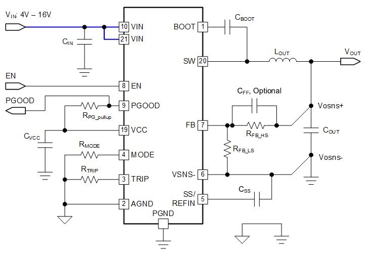
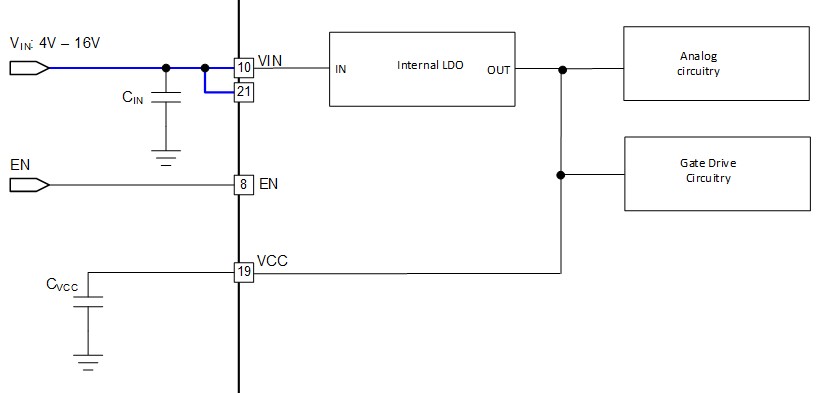
The input voltage of a DC/DC step-down converter is internally routed to analog circuitry, gate-drive circuitry, and the drain of the high-side MOSFET for power conversion. Since it is impractical and unnecessary to use a higher voltage semiconductor process for analog and gate-drive circuits, a separate internal LDO regulator is integrated into the DC/DC converter to provide power to these circuits. Figure 1-1 illustrates a typical DC/DC converter accepting a 4-V to 16-V input onto the VIN pins and Figure 1-2 shows an internal LDO providing power to the analog and gate-drive circuitry. The internal LDO powers all the analog circuitry and logic inside the IC, and its voltage may optimized for different voltage levels needed by the circuitry. The internal LDO steps-down the VIN voltage to the VCC voltage and the voltage-drop across the LDO causes power to be dissipated in the LDO. Since the load of the internal LDO is IVCC, the power dissipated by the internal LDO is (VIN – VLDO)*IVCC. A larger bias current and higher voltage-drop causes the DC/DC converter's efficiency to decrease.
 Figure 1-1 Typical DC/DC Converter with
Single Input Voltage
 Figure 1-2 DC/DC Converter with
Integrated Internal LDO