SNVAA08 October 2020 REF4132 , REF4132-Q1
4 Pin Failure Mode Analysis (Pin FMA)
This section provides a Failure Mode Analysis (FMA) for the pins of the REF4132-Q1. The failure modes covered in this document include the typical pin-by-pin failure scenarios:
- Pin short-circuited to Ground (see Table 4-2)
- Pin open-circuited (see Table 4-3)
- Pin short-circuited to an adjacent pin (see Table 4-4)
- Pin short-circuited to VIN (see Table 4-5)
Table 4-2 through Table 4-5 also indicate how these pin conditions can affect the device as per the failure effects classification in Table 4-1.
| Class | Failure Effects |
|---|---|
| A | Potential device damage that affects functionality |
| B | No device damage, but loss of functionality |
| C | No device damage, but performance degradation |
| D | No device damage, no impact to functionality or performance |
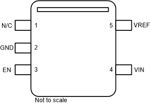
Figure 4-1 shows the REF4132-Q1 pin diagram. For a detailed description of the device pins please refer to the Pin Configuration and Functions section in the REF4132-Q1 data sheet.
 Figure 4-1 DBV Package5-Pin SOT-23Top View
Following are the assumptions of use and the device configuration assumed for the pin FMA in this section:
- Unless otherwise specified, the voltage applied to the VIN pin is within the REF4132-Q1 Recommended Operating Range.
- Device functionality indicates that the REF4132-Q1 output voltage is regulated
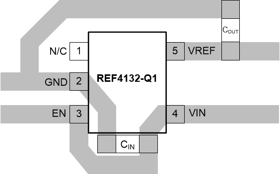
- Layout used for this analysis is given by Figure 4-2
 Figure 4-2 Layout
Example
Figure 4-2 Layout
Example| Pin Name | Pin No. | Description of Potential Failure Effect(s) | Failure Effect Class |
|---|---|---|---|
| N/C | 1 | Could affect functionality of device. Pin is not internally connected to GND. | B |
| GND | 2 | No Effect. | D |
| EN | 3 | Disables device, no output voltage, high leakage. | B |
| VIN | 4 | No output voltage, high leakage. | B |
| VREF | 5 | No output voltage. | B |
| Pin Name | Pin No. | Description of Potential Failure Effect(s) | Failure Effect Class |
|---|---|---|---|
| N/C | 1 | No Effect. | D |
| GND | 2 | No output voltage. | B |
| EN | 3 | Disables device, no output voltage. | B |
| VIN | 4 | Output is not regulated. | B |
| VREF | 5 | Output is not regulated. | B |
| Pin Name | Pin No. | Shorted to | Description of Potential Failure Effect(s) | Failure Effect Class |
|---|---|---|---|---|
| N/C | 1 | GND | Could affect functionality. Pin not internally connected to GND. | B |
| GND | 2 | EN | Disables device, no output voltage, high leakage. | B |
| EN | 3 | VIN | No Effect. | D |
| VIN | 4 | VREF | Output is not regulated, high leakage. | B |
| VREF | 5 | N/C | Could affect functionality. Pin not internally connected to GND. | B |
| Pin Name | Pin No. | Description of Potential Failure Effect(s) | Failure Effect Class |
|---|---|---|---|
| N/C | 1 | Could affect functionality of device. Pin is not internally connected to GND. | B |
| GND | 2 | No output voltage, high leakage. | B |
| EN | 3 | No Effect. | D |
| VIN | 4 | No Effect. | D |
| VREF | 5 | Output is not regulated, high leakage. | B |