SLVUC49 April 2021
7.3 Output Voltage Ripple
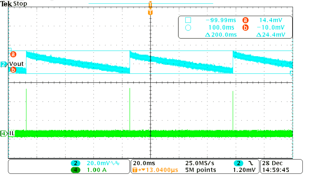
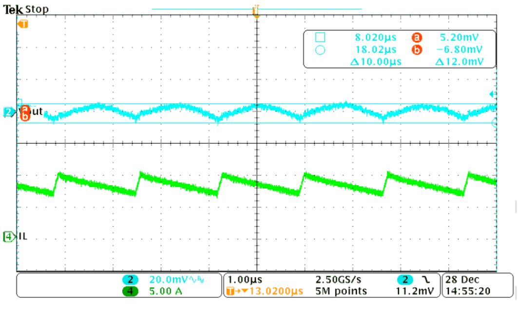
Figure 7-5 and Figure 7-6 show the output voltage ripple with 0 A and 8 A for the TPS51396AEVM board. The input voltage is 12 V.
 Figure 7-5 Output Ripple with 0 A Loading at ECO Mode
 Figure 7-6 Output Ripple with 8 A Loading at ECO Mode
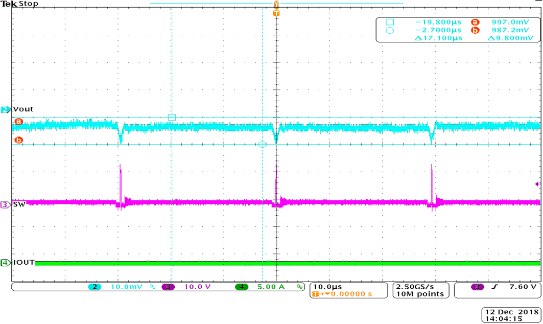
Figure 7-7 shows the output voltage ripple with 0-A loading at OOA mode. Input voltage is 12 V.
 Figure 7-7 Output Ripple with 0 A at OOA Mode