SLVAF68 July 2021 TPS61086
1 Introduction
The Boost converter is used to step-up an input voltage to some higher level, and this characteristic is achieved by storing energy in an inductor and releasing it to the load at a higher voltage. The TPS61086 device that is specifically designed for Boost converter applications allows the use of small external inductors and capacitors with high switching frequency (1.2 MHz) and provides fast transient response.
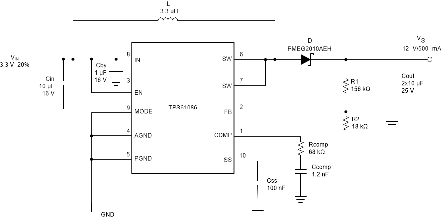
Figure 1-1 shows the typical application circuit of the TPS61086 to get 12-V output from 3.3-V input. As shown in Figure 1-1, the typical application for the TPS61086 is to reach higher level of positive output voltage from positive input voltage using the Boost topology as it is the primary intended application. However, if a negative voltage is available in the system, it is necessary to use the negative voltage as the input for the converter, and it is beneficial to create more negative amplitude directly from the negative input voltage in non-isolated DC-to-DC solutions including point-of-load applications.
 Figure 1-1 Typical Application Circuit of the
TPS61086
Figure 1-1 Typical Application Circuit of the
TPS61086It is certainly important to understand not only the internal construction of the TPS61086 itself but also switcher topologies themselves for the conversion across different topologies. There are many things to consider working on new configurations including voltage ratings of each pin, the feedback path, the ground connection and so on, and these are essential to get the desired results.