SLVAF43 May 2021 TPS65235 , TPS65235-1 , TPS652353
1 Introduction
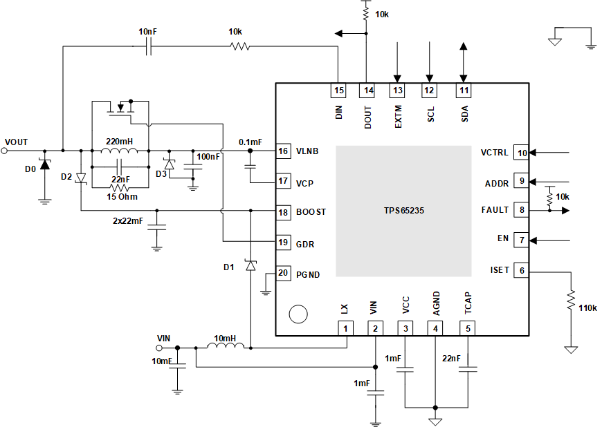
The DiSEqC™ 2.x protocol supports two way communications for receiver or controller and accessory or peripheral modes. Figure 1-1 shows a typical DiSEqC 2.x implementation using TPS65235.
 Figure 1-1 Typical DiSEqC™ 2.x Implementation
In accessory or peripheral mode a 22-kHz tone is received at VOUT. The tone is blocked from reaching VLNB by the LCR filter. This is a band stop filter presenting 15-Ω impedance at 22 kHz. The tone is passed via the 10 nF, 10-kΩ RC filter to the DIN pin. The DC current for the LNB power flows from VLNB to VOUT via the 220-µH inductor which has low DC resistance.
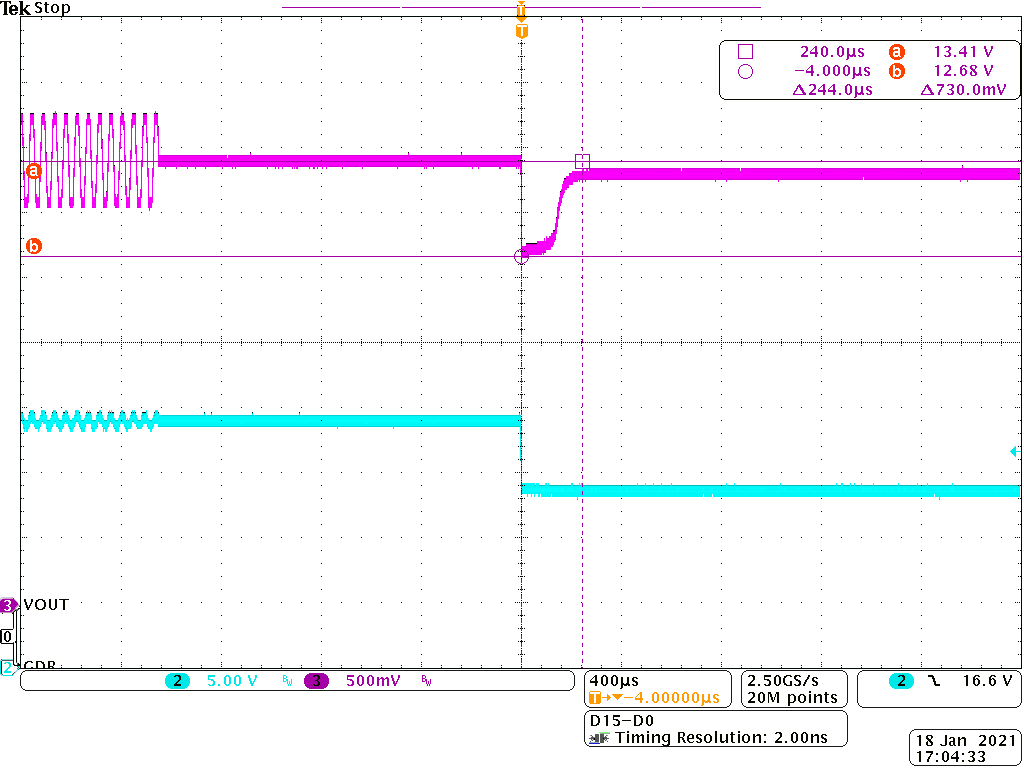
In receiver or controller mode, the LNB power supply transmits a 22-kHz tone on VOUT. When transmitting, a FET is turned on to bypass the LCR filter and avoid unwanted attenuation of the 22-kHz tone. The lowest resistance DC path is through this FET when on. However, when the FET is turned off, the current cannot ramp instantly in the inductor and initially the current flows through the 15-Ω resistor. The voltage dropped across the resistor leads to a sudden drop or negative spike in the VOUT signal, which subsequently decreases as the inductor current ramps. For a 600-mA LNB current, the drop across the resistor could be as high as 9 V but it is clamped at approximately 700 mV by the body diode of the FET as seen in Figure 1-2. This negative spike can be incorrectly interpreted by some LNBs and can lead to incorrect communication and missed commands.
 Figure 1-2 Negative Voltage Spike Clamped to Approximately 700 mV by FET Body Diode