SLVAF11 June 2021 TPS51397A , TPS566231 , TPS566235 , TPS566238 , TPS568230
4 Example of LC Design Method for D-CAP3 Converter
TPS568230 is used as the example. Vin=12V, Vo=1.5V, fsw=600kHz, Ioutmax=8A.
First, choose inductance to let the inductor current ripple equal to 20%-40% of max loading current. The inductance value can be derived as Equation 21.
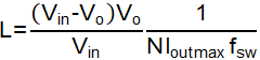
Substituting the parameters into Equation 21, it can be calculated that 0.68uH< L<1.36uH. Choose L=1uH. Choose inductor 744311100 and its DCR is 4.6mOhm. Substituting inductance and DCR into Equation 11 and Equation 15, we can get the range of output capacitance as 35uF< Co<163uF.
Choose output capacitance Co=110uF. Here 5 parallel 22uF MLCC with 10V rated voltage are used and ESR of each one is about 3mohm. The total ESR is 0.6mohm.
For the estimation of phase margin and crossover frequency, the degrading of inductor and capacitor needs to be considered. With only 1.5 V DC bias, the degrading of output capacitor can be ignored. Degrading curve of inductance with increasing current is shown in Figure 4-1. The inductance is about 0.86uH at 8A loading.
 Figure 4-1 Degrading Curve of Inductance with
Increasing Current
Figure 4-1 Degrading Curve of Inductance with
Increasing CurrentIt can be calculated that the crossover frequency is 77kHz according to Equation 14 and phase margin is 57.7 degree according to Equation 19.
The application design method can be concluded as the flow chart in Figure 4-2.