SLVAEZ4 June 2021 TPS272C45
1 Basic Interaction
The TPS272C45EVM is equipped with BoosterPack headers to allow for easy interaction with a Texas Instruments microcontroller. While the BoosterPack headers enable easy interaction with a Texas Instruments branded microcontroller, any microcontroller with basic GPIO functionality and an ADC interface can be used. The relevant signals that can be controlled from the microcontroller are listed in Table 1-1.
| BoosterPack Pin | Function | Note |
|---|---|---|
| J1-1 | 3.3 V Power Rail | Disconnect J19 if powering LaunchPad through USB. |
| J1-2 | Current sensing through the SNS pin | Populate a Zener diode on D7 if it is required to limit analog signal of pin |
| J1-5 | DIA_EN pin used to enable diagnostics | Can be used to multiplex multiple TPS272C45 switches to one analog pin |
| J1-8 | SEL pin used to change measurement reported on SNS pin | |
| J2-11 | LATCH pin used to change fault behavior | |
| J2-12 | ILIM1 pin used to enable 10kΩ resistor R13 for ILIM1 | Active high. Do not enable at same time as J2-13 |
| J2-13 | ILIM2 pin used to enable 4.99kΩ resistor R14 for ILIM1 | Active high. Do not enable as same time as J2-12 |
| J2-17 | FLT pin used to detect faults | Open drain input. Pull-up source can be controlled using jumper J18 |
| J2-18 | EN2 to enable VOUT2 | Active high. Can be connected to PWM |
| J2-19 | EN1 to enable VOUT1 | Active high. Can be connected to PWM |
| J2-20 | Module GND | Do not connect to IC ground if ground network is used |
Note that before the TPS272C45 can be used with the MSP-EXP430F5529LP, the jumpers on the EVM must be configured to work in microcontroller mode. By default the TPS272C45EVM is configured to be used as a standalone EVM so the following jumper configurations must be made to route the relevant signals to the connected LaunchPad:
- Disconnect jumpers J8, J9, J10, J11, J12. These will allow the microcontroller to control the digital signal pins without any interaction from the LDO or ground
- Disconnect jumper J13. This will disable the onboard 3.3 V LDO
- Disconnect J14 and J15. This will allow the MSP430 to control the multiplexed current limit
- Configure J17 to the BP configuration. This will power the VDD rail through the LaunchPad's 3.3 V signal
- Configure J18 to the BP configuration. This will pull the FAULT pin up through the LaunchPad's 3.3 V signal
A simple code example that shows the basic setup of the TPS272C45 can be found in the tps272c45_basic_setup folder of the source package included with this application note. In this code example the DIAG_EN, SEL, LATCH, and EN1/EN2 lines are setup as outputs, the FLT line is set as an interruptible input. The SNS pin is not used in this application. The S1 and S2 push buttons on the MSP-EXP430F5529LP are used in this application to toggle EN1 and EN2 on and off respectively. This is simply done by toggling the output state of the GPIO in each button’s interrupt handler. The interrupt handlers for the S1/EN1 interrupt handler are shown here:
#pragma vector=PORT2_VECTOR
__interrupt void Port_2(void)
{
    switch (__even_in_range(P2IV, 16))
    {
        case P2IV_NONE:
            break;   // Vector  0: no interrupt
        case P2IV_P2IFG0:
            break;   // Vector  2: P2.0
        case P2IV_P2IFG1:
            P1OUT ^= BIT0;    // Vector  4: P2.1 (EN1)
            en1On = !en1On;
            EN1_OUT ^= EN1_PIN;
            break;
        case P2IV_P2IFG2:
            break;   // Vector  6: P2.2
        case P2IV_P2IFG3:
            break;   // Vector  8: P2.3
        case P2IV_P2IFG4:
            break;   // Vector 10: P2.4
        case P2IV_P2IFG5:
            break;   // Vector 12: P2.5
        case P2IV_P2IFG6:
            break;   // Vector 14: P2.6
        case P2IV_P2IFG7:
            break;   // Vector 16: P2.7
        default:
            break;
    }
}
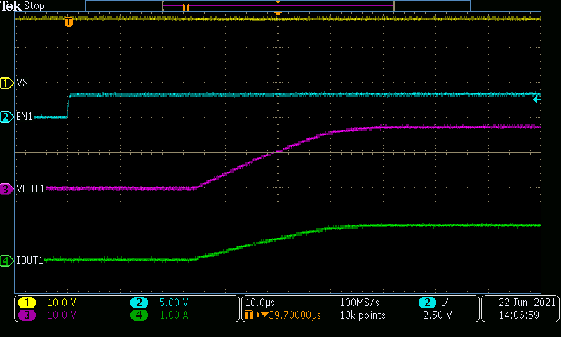
The oscilloscope screenshot of the TPS272C45 with an 18 V supply hooked up to an 18Ω load when EN1 is pressed can be shown in Figure 1-1:
 Figure 1-1 Output Toggling
When the EN1 channel is ON the green LED on the LaunchPad will be turned on and when the EN2 channel is ON the red LED of the LaunchPad will be turned on. Also note that when a fault occurs in the system (as detected with the FLT line) the LaunchPad's LEDs will blink quickly to illustrate the fault. The fault is detected in the software by setting up an edge triggered GPIO interrupt on the FLT line. When the fault is resolved the microcontroller will detect the rising edge on the fault line and resume normal LED behavior. Note that the FLT line must be pulled up to the logic level of the microcontroller by either an internal pull up in the microcontroller or an external pull-up. The interrupt handler for the fault line in the case of an over current event are shown here:
#pragma vector=PORT1_VECTOR
__interrupt void Port_1(void)
{
    switch (__even_in_range(P1IV, 16))
    {
        case P1IV_NONE:
            break;   // Vector  0: no interrupt
        case P1IV_P1IFG0:
            break;   // Vector  2: P1.0
        case P1IV_P1IFG1:
            P4OUT ^= BIT7;    // Vector  4: P1.1 (EN2)
            en2On = !en2On;
            EN2_OUT ^= EN2_PIN;
            break;
        case P1IV_P1IFG2:
            break;   // Vector  6: P1.2
        case P1IV_P1IFG3:
            break;   // Vector  8: P1.3
        case P1IV_P1IFG4:
            FAULT_IE &= ~FAULT_PIN;   // Vector 10: P1.4 (Fault)
            TA0CTL = TASSEL_2 + MC_1 + TACLR;
            break;
        case P1IV_P1IFG5:
            break;   // Vector 12: P1.5
        case P1IV_P1IFG6:
            break;   // Vector 14: P1.6
        case P1IV_P1IFG7:
            break;   // Vector 16: P1.7
        default:
            break;
    }
}