SLVAER2A April 2020 – November 2020 TPS50601-SP , TPS50601A-SP
3 Schematic and Layout Changes
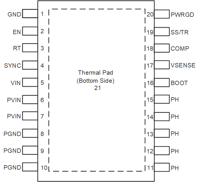
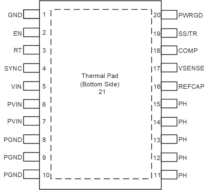
Most designs will need very little change to upgrade from the TPS50601-SP. The package pictures of the devices are shown in Figure 3-1 and Figure 3-2. While the devices are mechanically the same, pin 16 is different between the two devices. The TPS50601-SP has pin 16 as a bootstrap pin for the high-side nFET, and the TPS50601A-SP has a pin to place a capacitor to help stabilize the reference voltage. For layout, the TPS50601-SP requires a 0.1-μF ceramic capacitor to be placed between the pin and the PH node, while the TPS50601A-SP requires a 470-μF ceramic capacitor from the pin to ground. If all the component value changes have a comparable footprint, this is the only layout change needed between the two devices.
 Figure 3-1 TPS50601-SP Pin Out
Diagram
 Figure 3-2 TPS50601A-SP Pin Out
Diagram