SLVA267B Mar 2007 – September 2018 MSP430F427 , TLC5940 , TLC5940-EP , TLC5941
2 TLC5941 Driver Implementation Using the MSP430F427
Figure 5 and Figure 6 show the schematic of the hardware for the implementation of the circuit with the MSP430F427 and TLC5941. The schematic shows the MSP430F427, the TLC5941, and power circuits needed to implement a complete 16-LED display drive. Additional TLC5941s can be cascaded on the serial communication bus to accommodate any number of LEDs.
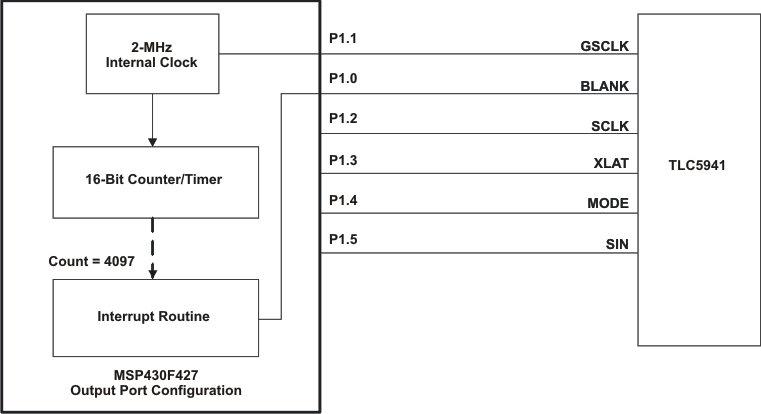
The hardware is configured so that the TLC5941 is controlled by six general-purpose I/O (GPIO) pins on the MSP430F427. All six of these GPIO pins are configured as outputs on port one of the MSP430F427. One output pin (P1.1) is configured to be driven by the internal system clock of the MSP430™ MCU. This output pin drives the GSCLK of the TLC5941. The system clock, internal to the MSP430F427, also supplies the clock to a 16-bit counter which also is internal to the MSP430F427. The counter is configured to count from 0 to 4097 with each clock pulse. When the counter reaches 4097, it generates an interrupt. An interrupt routine then pulses the output bit that connects to the BLANK signal of the TLC5941. Figure 1 shows a simplified block diagram of this clocking scheme. This clocking scheme makes the GSCLK and BLANK signal generation transparent to the rest of the software. The firmware only needs to send dot correction and grayscale data to drive the LEDs.
 Figure 1. Simplified Block Diagram Of Clocking Scheme
 Figure 2 shows a flow chart for the main loop of the firmware. The major portions of the communications firmware resides in three subroutines which makes the main loop very simple. The main loop simply initializes the output port, turns off the watchdog timer and configures the counter. Once these initialization steps are complete, the main loop simply sends all of the dot correction and grayscale data stored in RAM to the TLC5941 and then enters an infinite loop. The main loop ends in an infinite loop instead of halting the processor so that the interrupt routines continue to operate and drive the LEDs.
The GSOUT routine is used to send all of the grayscale data stored in RAM to the TLC5941. The 12-bit grayscale data is stored in RAM as left-justified, 16-bit words. Therefore, the lower four bits of each grayscale data in RAM are ignored by the firmware and are not sent to the TLC5941.
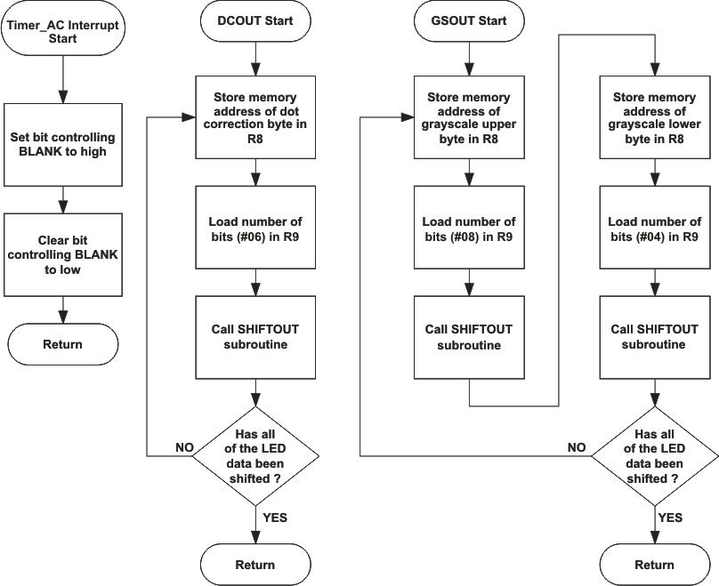
The DCOUT routine is used to send all of the dot correction data stored in RAM to the TLC5941. The 6-bit dot correction data is stored in RAM as left-justified, 8-bit bytes. Therefore, the lower two bits of each dot correction data in RAM are ignored by the firmware and are not sent to the TLC5941. Figure 3 shows the flow charts for the interrupt, GSOUT, and GSOUT routines
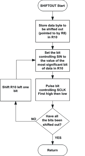
The GSOUT and DCOUT routines are similar and could be combined, together with the addition of some flags and conditional statements. This was not done for this example to clarify the difference between grayscale and dot correction communications. Both of these routines determine which byte of data in RAM is to be sent, how many bits of that byte are to be sent, and then passes these two parameters to the SHIFTOUT subroutine. The SHIFTOUT subroutine simply takes the byte of data and drives the bits of the output port that drive the serial communication pins of TLC5941. Figure 4 is the flow chart for the SHIFTOUT subroutine.
 Figure 2. Main Loop Flow Chart
  Figure 3. Interrupt and Subroutine Flow Charts
  Figure 4. SHIFTOUT Flow Chart