SLUUCF9A March   2021  – April 2021 TPS566231 , TPS566238


  1.   Trademarks
  2. 1Introduction
  3. 2Performance Specification Summary
  4. 3Output Voltage Setpoint
  5. 4Test Setup and Results
    1. 4.1 Input/Output Connections
    2. 4.2 Start-Up Procedure
    3. 4.3 Start-Up
    4. 4.4 Shut-Down
    5. 4.5 Output Voltage Ripple
  6. 5Board Layout
    1. 5.1 Layout
  7. 6Board Profile, Schematic, List of Materials, and Reference
    1. 6.1 Board Profile
    2. 6.2 Schematic
    3. 6.3 List of Materials
    4. 6.4 Reference
  8. 7Revision History

Board Profile

Figure 6-1 is the top view for the TPS566231PEVM.
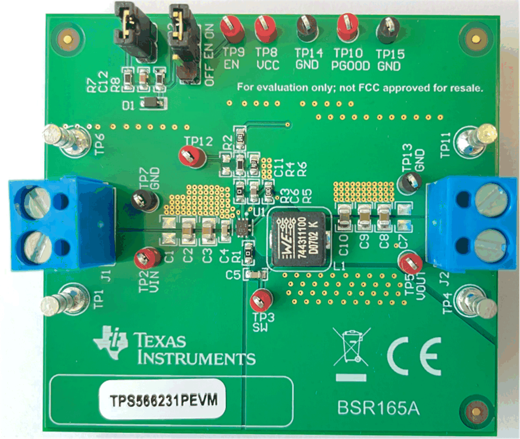
GUID-20210301-CA0I-MRHH-8XJ2-WH0B528B1WM8-low.gif Figure 6-1 Top View of TPS566231PEVM

Figure 6-2 is the bottom view for the TPS566231PEVM.
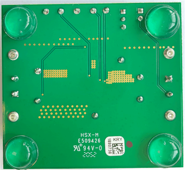
GUID-20210301-CA0I-G7GP-PQPQ-KX79RRNCBX38-low.gif Figure 6-2 Bottom View of TPS566231PEVM