SLUUC04A February 2019 – June 2021
6.3 Output Voltage Ripple
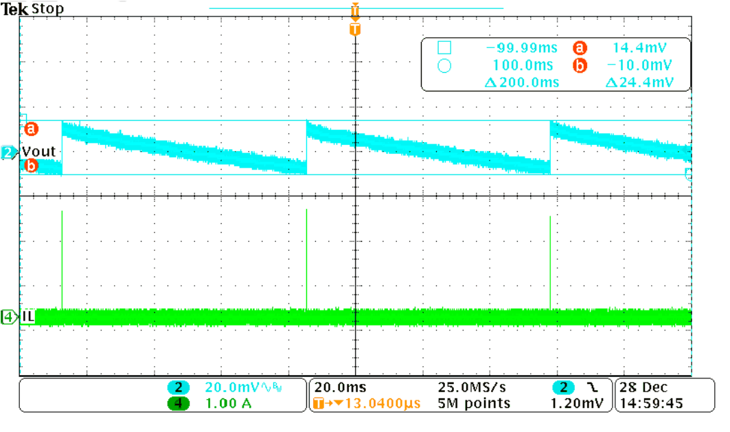
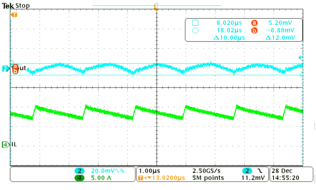
Figure 6-5 and Figure 6-6 show the output voltage ripple with 0 A and 8 A for the TPS568230EVM board. The input voltage is 12 V.
 Figure 6-5 Output Ripple with 0 A Loading at ECO Mode
 Figure 6-6 Output Ripple with 8 A Loading at ECO Mode
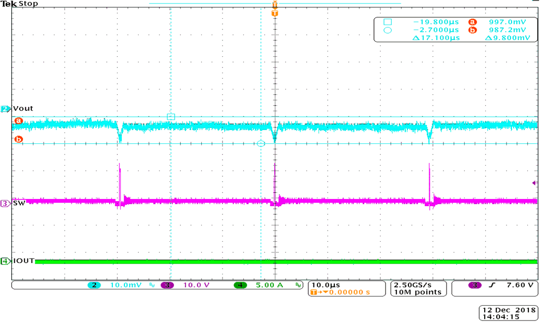
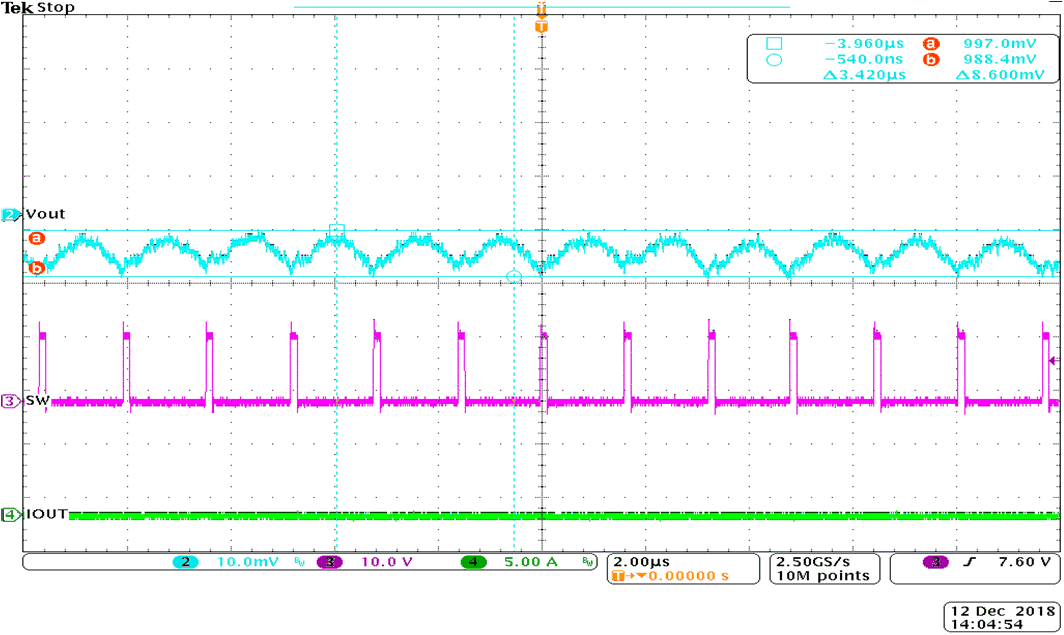
Figure 6-7 and Figure 6-8 show the output voltage ripple with 0-A loading at OOA mode and FCCM mode. Input voltage is 12 V.
 Figure 6-7 Output Ripple with 0 A at OOA Mode
 Figure 6-8 Output Ripple with 0 A at FCCM Mode