SLUS670C JULY 2005 – January 2015 TPS51120
PRODUCTION DATA.
- 1 Features
- 2 Applications
- 3 Description
- 4 Revision History
- 5 Pin Configuration and Functions
- 6 Specifications
-
7 Detailed Description
- 7.1 Overview
- 7.2 Functional Block Diagram
- 7.3
Feature Description
- 7.3.1 PWM Operation
- 7.3.2 Adaptive On-Time Control
- 7.3.3 Light Load Operation
- 7.3.4 Forced PWM Operation
- 7.3.5 5-V, 100-mA, LDO and Switchover (VREG5)
- 7.3.6 3.3-V, 100-mA, LDO and Switchover (VREG3)
- 7.3.7 2-V, 50-uA Sink - Source Reference (VREF2)
- 7.3.8 Low-Side Driver
- 7.3.9 High-Side Driver
- 7.3.10 Soft-Start
- 7.3.11 Soft-Stop
- 7.3.12 Powergood
- 7.3.13 Current Sensing and Overcurrent Protection
- 7.3.14 Overvoltage Protection
- 7.3.15 Undervoltage Protection
- 7.3.16 5-V Supply and UVLO Protection
- 7.3.17 VIN Line Sag Protection (Dynamic UVP)
- 7.3.18 Thermal Shutdown
- 7.4 Device Functional Modes
- 7.5 Programming
- 8 Application and Implementation
- 9 Power Supply Recommendations
- 10Layout
- 11Device and Documentation Support
- 12Mechanical, Packaging, and Orderable Information
8 Application and Implementation
NOTE
Information in the following applications sections is not part of the TI component specification, and TI does not warrant its accuracy or completeness. TI’s customers are responsible for determining suitability of components for their purposes. Customers should validate and test their design implementation to confirm system functionality.
8.1 Application Information
The TPS51120 is typically used as a dual-synchronous buck controller, which convert an input voltage ranging from 4.5V to 28 V, to output voltage ranging 1V to 5.5 V, targeted for notebook I/O and low voltage system bus supply solutions.
8.2 Typical Application
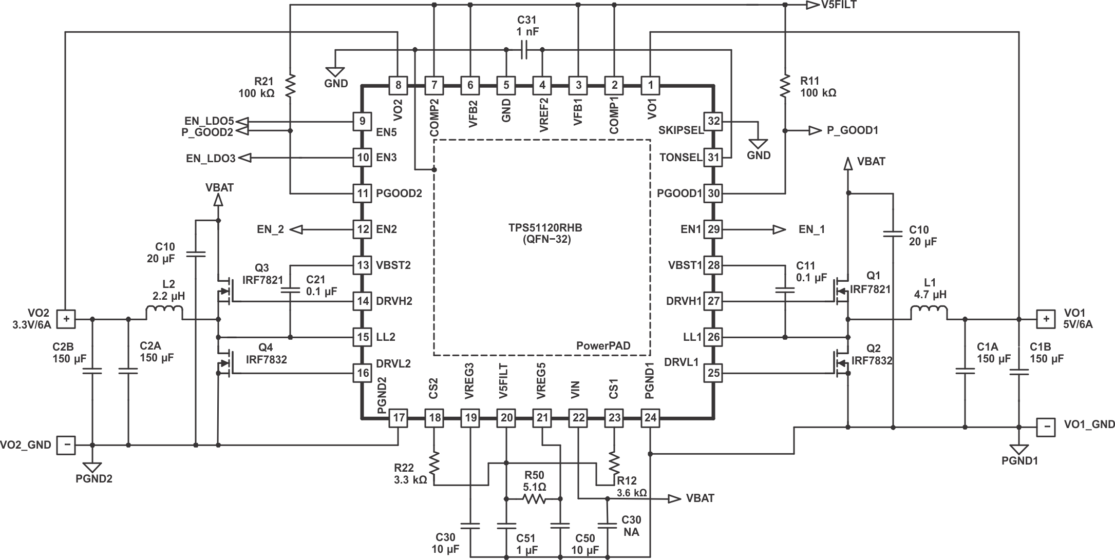 Figure 32. D-Cap Mode, Fixed 5-V / 6-A, 3.3-V/6-A, RDS(on) Sensing
8.2.1 Design Requirements
Table 6. Design Parameters
| DESIGN PARAMETER | VALUE | |||
|---|---|---|---|---|
| Input Voltage Range | 4.5 V to 28 V | |||
| Channel 1 Output Voltage | 5 V | |||
| Channel 1 Output Current | 6 A | |||
| Channel 2 Output Voltage | 3.3 V | |||
| Channel 2 Output Current | 6 A | |||
8.2.2 Detailed Design Procedure
- Determine output voltage. Since 5 V and 3.3 V is the default fixed output voltage, tie VFB1 and VFB2 to V5FILT to choose the internal feedback resistor divider.
- Choose control mode. Tie COMP1 and COMP2 to V5FILT to choose D-CAP control mode.
- Choose switching frequency. Tie TONSEL to VREF2, choose 280kHz/430kHz for channel1 and channel2 respectively.
- Choose the inductor. To make the inductor ripple current at ½ of maximum output current, calculate inductance according to Equation 12 as below:
- Choose the output capacitor. To get an acceptable jitter level, approximately 15mV ripple at comparing point is needed. Refer to Equation 20. This require the minimum ESR of output capacitors for channel1 and channel2 is:
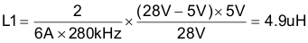
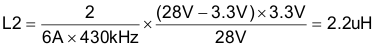
4.7-uH and 2.2-uH inductor is chosen for channel1 and channel2 respectively. Check inductor specification, make sure the saturation current is higher than peak inductor current in this application with enough room.
Choose 2pcs 150-uF/50-mΩ SP-CAP in parallel, the equivalent capacitance and ESR is 300 uF and 25 mΩ, meet above requirement.
0dB frequency f0 calculated as below:
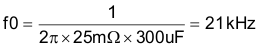
F0 is much less than 1/3 of the switching frequency, loop should be stable.
8.2.3 Application Curves
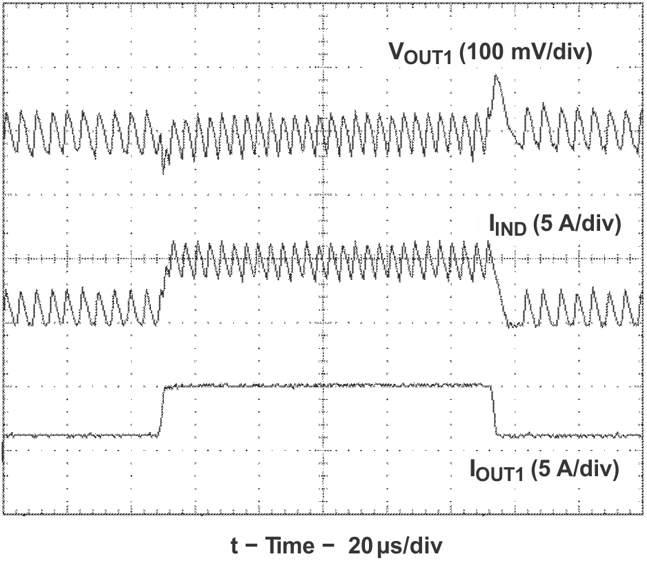 Figure 33. 5-V Load Transient Response
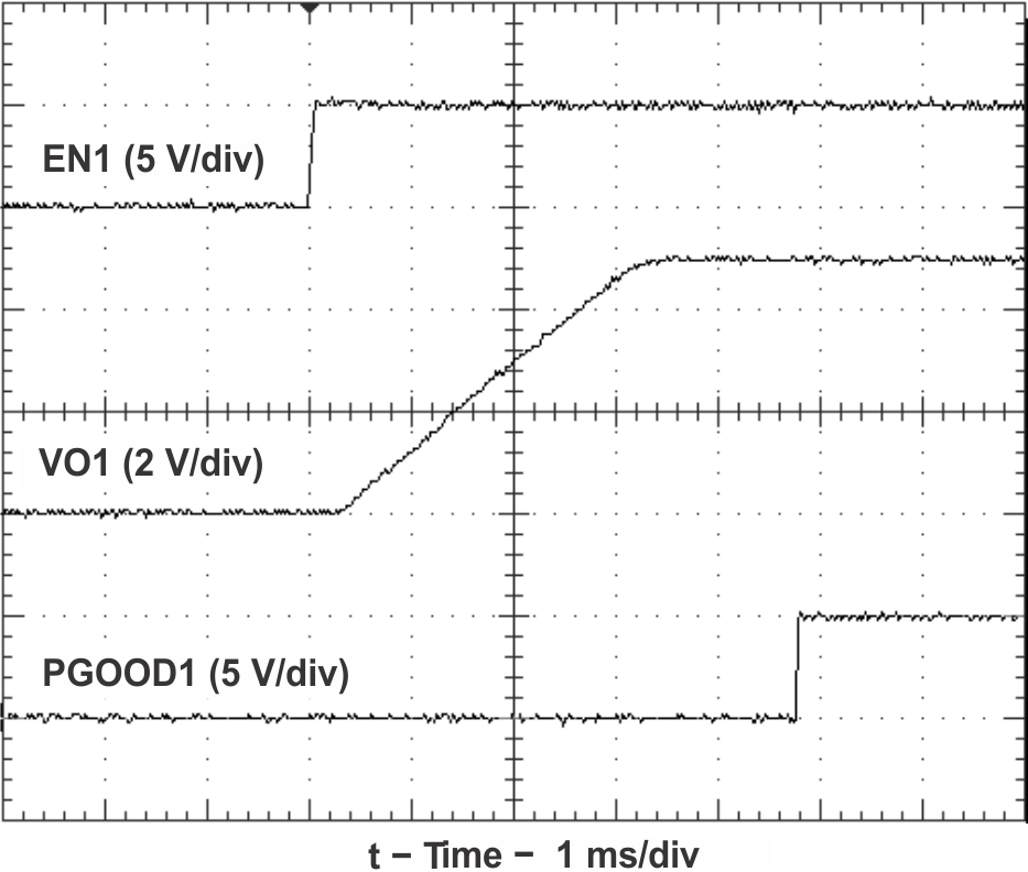 Figure 35. 5-V Startup Waveforms
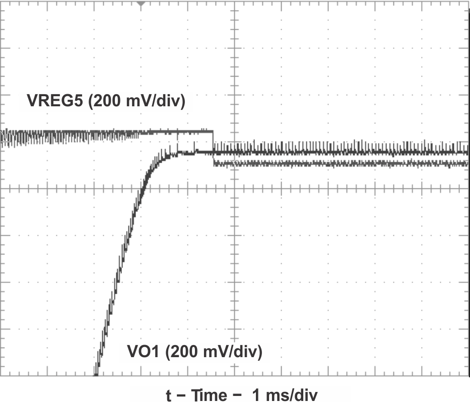 Figure 37. 5-V Switchover Waveforms
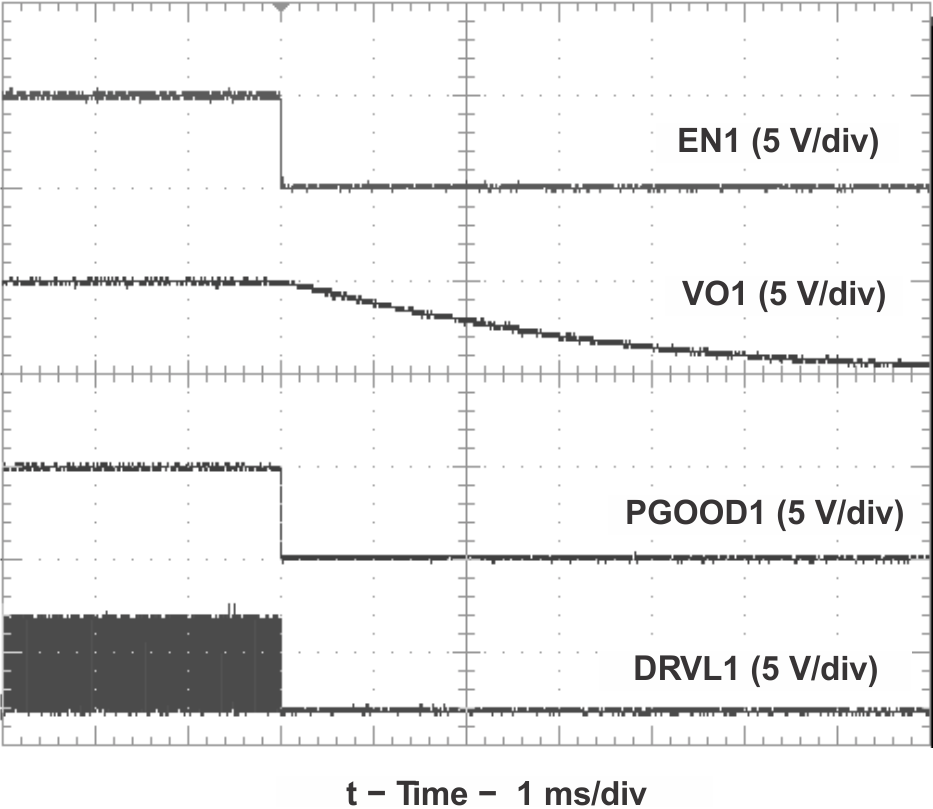 Figure 39. 5-V Soft-Stop Waveforms
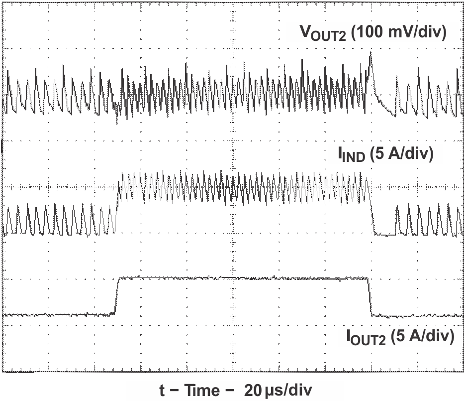 Figure 34. 3.3-V Load Transient Response
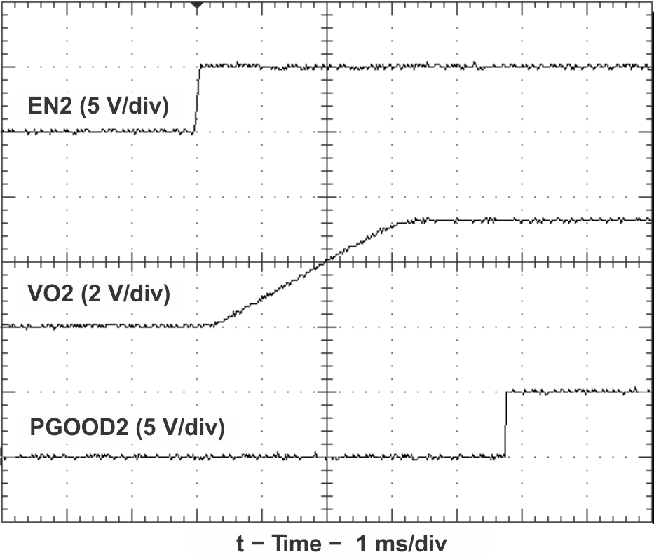 Figure 36. 3.3-V Startup Waveforms
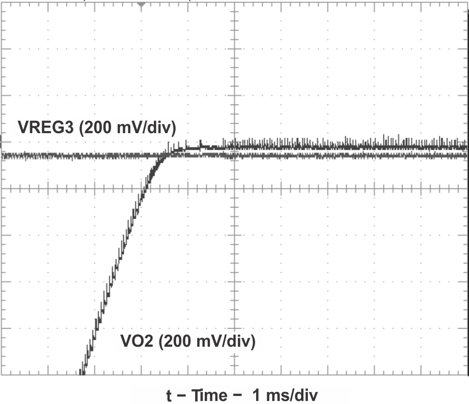 Figure 38. 3.3-V Switchover Waveforms
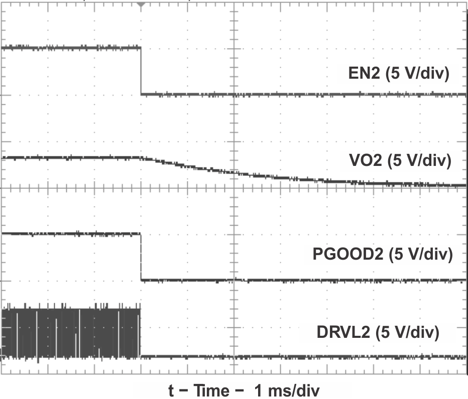 Figure 40. 3.3-V Soft-Stop Waveforms