SLUA749A July 2015 – May 2016 BQ76920 , BQ76930 , BQ76940
3 Device Architecture
The bq769x0 family devices are built with a 5 cell group structure. Each cell group can support 3 to 5 cells. Each group has a 14-bit ADC which supports its 5 cells and thermistor. Each group has an independent timeline. Voltage and temperature readings from the upper groups are communicated to the bottom group registers for access by the host. Power for the voltage and temperature circuit comes from the BAT pin. Current monitoring, FET drives, and user communication are provided only on the bottom group, power for these functions comes from the REGSRC pin.
The bq76920 uses a single cell group. Signals are referenced to VSS. The bq76920 BAT pin can be powered by a hold-up circuit so that a moderately sized filter capacitor can be used. A method to prevent excessive voltage on the pin should be provided; a discharge resistor across the diode may prove sufficient. In some cases a zener may be needed to limit the voltage on the pin. The zener should limit the voltage to a few volts above the top cell. The Rc and Cc input filter components used with the bq76920 can use a wide range of values.
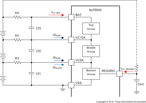
The bq76930 and bq76940 stack 5 cell groups using 2 and 3 groups, respectively. The VSS of the upper group is connected to the BAT pin of the lower group. The supply current flows from the BAT pin through each group to VSS. Only a small offset current flows in the intermediate power pins (VC5X and VC10X), this is shown in Figure 2, values are shown in the datasheet. There is an offset current increase into VC5X when the ALERT signal is high, the accumulative effect of this current on the system can be minimized by the microcontroller clearing the status register as soon as the ALERT is set.
 Figure 2. BAT Supply and Offset Currents
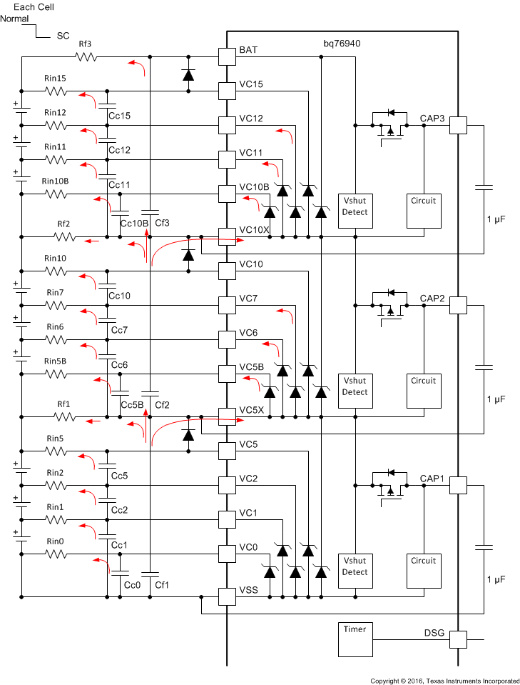
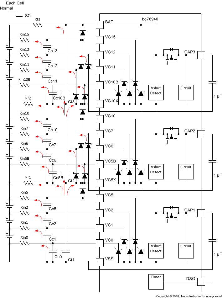
 With this device architecture of the bq76930 and bq76940, when a heavy load such as a short circuit is applied to the battery, each cell voltage will drop to a low value. Current is drawn through each input filter resistor. Initially the filter capacitors discharge. On the lower group the inputs do not go below VSS. On the upper groups, the Cf power filter capacitors hold the group reference voltage above battery- and current continues to flow from the input resistors. After the input filter capacitors are depleted, current will flow from the device inputs continuing the discharge of the lower Cf capacitors as shown in Figure 3. This current flow is generally undesired in semiconductor devices but the family was designed with this architecture. The input voltage will drop below the group reference, but current is limited by the input resistors and no damage is expected. If needed for the individual implementation, Schottky diodes may be connected from the group reference to the group inputs to carry the current outside the device. These diodes are shown in Figure 4 and patterns were included on the EVM. The BAT pin filter resistor draws current through the stack of Cf capacitors. The upper group inputs draw current from the lower group’s Cf capacitor. The upper Cf capacitor will discharge more slowly than the lower Cf capacitor. The lower group power must remain above the VSHUT level so that the device can time the short circuit event and turn off the DSG FET output.
 Figure 3. Current From Input Pins
  Figure 4. Avoiding Pin Current With Schottky Diodes
 Because of the architecture of the bq76930 and bq76940, the Cf capacitors used should be large and the input filter resistors should also be large. Generally the Cf capacitors use the same value for all capacitors. A hold-up circuit with diodes should not be used on the power pins of the bq76930 and bq76940. The datasheet shows a large range of values, but the larger values should be used with these family members.