• Menu
  • Product
  • Email
  • PDF
  • Order now
  • TPA6130A2 138-mW DIRECTPATH™ Stereo Headphone Amplifier with I2C Volume Control

    • SLOS488F November   2006  – March 2015 TPA6130A2

      PRODUCTION DATA.  

  • CONTENTS
  • SEARCH
  • TPA6130A2 138-mW DIRECTPATH™ Stereo Headphone Amplifier with I2C Volume Control
  1. 1 Features
  2. 2 Applications
  3. 3 Description
  4. 4 Simplified Schematic
  5. 5 Revision History
  6. 6 Pin Configuration and Functions
  7. 7 Specifications
    1. 7.1 Absolute Maximum Ratings
    2. 7.2 Handling Ratings
    3. 7.3 Recommended Operating Conditions
    4. 7.4 Thermal Information
    5. 7.5 Electrical Characteristics
    6. 7.6 Operating Characteristics
    7. 7.7 Timing Requirements
    8. 7.8 Typical Characteristics
  8. 8 Detailed Description
    1. 8.1 Overview
    2. 8.2 Functional Block Diagram
    3. 8.3 Feature Description
      1. 8.3.1 Headphone Amplifiers
    4. 8.4 Device Functional Modes
      1. 8.4.1 Hardware Shutdown
      2. 8.4.2 Software Shutdown
      3. 8.4.3 Charge Pump Enabled, HP Amplifiers Disabled
      4. 8.4.4 Hi-Z State
      5. 8.4.5 Stereo Headphone Drive
      6. 8.4.6 Dual Mono Headphone Drive
      7. 8.4.7 Bridge-Tied Load Receiver Drive
      8. 8.4.8 Default Mode
      9. 8.4.9 Volume Control
    5. 8.5 Programming
      1. 8.5.1 General I2C Operation
      2. 8.5.2 Single-and Multiple-Byte Transfers
      3. 8.5.3 Single-Byte Write
      4. 8.5.4 Multiple-Byte Write and Incremental Multiple-Byte Write
      5. 8.5.5 Single-Byte Read
      6. 8.5.6 Multiple-Byte Read
    6. 8.6 Register Maps
      1. 8.6.1 Control Register (Address: 1)
      2. 8.6.2 Volume and Mute Register (Address: 2)
      3. 8.6.3 Output Impedance Register (Address: 3)
      4. 8.6.4 I2C address and Version Register (Address: 4)
      5. 8.6.5 Reserved for test registers (Addresses: 5-8)
  9. 9 Applications and Implementation
    1. 9.1 Application Information
    2. 9.2 Typical Application
      1. 9.2.1 Design Requirements
      2. 9.2.2 Detailed Design Procedure
        1. 9.2.2.1 Input-Blocking Capacitors
        2. 9.2.2.2 Charge Pump Flying Capacitor and CPVSS Capacitor
        3. 9.2.2.3 Decoupling Capacitors
        4. 9.2.2.4 I2C Control Interface Details
          1. 9.2.2.4.1 Addressing the TPA6130A2
        5. 9.2.2.5 Headphone Amplifiers
      3. 9.2.3 Application Performance Curves
  10. 10Power Supply Recommendations
  11. 11Layout
    1. 11.1 Layout Guidelines
    2. 11.2 Layout Example
  12. 12Device and Documentation Support
    1. 12.1 Trademarks
    2. 12.2 Electrostatic Discharge Caution
    3. 12.3 Glossary
  13. 13Mechanical, Packaging, and Orderable Information
  14. IMPORTANT NOTICE
search No matches found.
  • Full reading width
    • Full reading width
    • Comfortable reading width
    • Expanded reading width
  • Card for each section
  • Card with all content


DATA SHEET

TPA6130A2 138-mW DIRECTPATH™ Stereo Headphone Amplifier with I2C Volume Control

1 Features

  • DirectPath™ Ground-Referenced Outputs
    • Eliminates Output DC Blocking Capacitors
    • Reduces Board Area
    • Reduces Component Height and Cost
    • Full Bass Response Without Attenuation
  • Power Supply Voltage Range: 2.5 V to 5.5 V
  • 64 Step Audio Taper Volume Control
  • High Power Supply Rejection Ratio
    (>100 dB PSRR)
  • Differential Inputs for Maximum Noise Rejection (68 dB CMRR)
  • High-Impedance Outputs When Disabled
  • Advanced Pop and Click Suppression Circuitry
  • Digital I2C Bus Control
    • Per Channel Mute and Enable
    • Software Shutdown
    • Multi-Mode Support: Stereo HP, Dual Mono HP, and Single-Channel BTL Operation
    • Amplifier Status
  • Space Saving Packages
    • 20 Pin, 4 mm x 4 mm QFN
    • 16 ball, 2 mm x 2 mm DSBGA
  • ESD Protection of 8 kV HBM and IEC Contact

2 Applications

  • Mobile Phones
  • Portable Media Players
  • Notebook Computers
  • High Fidelity Applications

3 Description

The TPA6130A2 is a stereo DirectPath™ headphone amplifier with I2C digital volume control. The TPA6130A2 has minimal quiescent current consumption, with a typical IDD of 4 mA, making it optimal for portable applications. The I2C control allows maximum flexibility with a 64 step audio taper volume control, channel independent enables and mutes, and the ability to configure the outputs into stereo, dual mono, or a single receiver speaker BTL amplifier that drives 300 mW of power into 16 Ω loads.

The TPA6130A2 is a high fidelity amplifier with an SNR of 98 dB. A PSRR greater than 100 dB enables direct-to-battery connections without compromising the listening experience. The output noise of 9 μVrms (typical A-weighted) provides a minimal noise background during periods of silence. Configurable differential inputs and high CMRR allow for maximum noise rejection in the noisy environment of a mobile device.

TPA6130A2 packaging includes a 2 by 2 mm chip-scale package, and a 4 by 4 mm QFN package.

Device Information(1)

PART NUMBER PACKAGE BODY SIZE (NOM)
TPA6130A2 WQFN (20) 4.00mm x 4.00mm
DSBGA (16) 2.00mm x 2.00mm
  1. For all available packages, see the orderable addendum at the end of the datasheet.

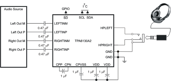
4 Simplified Schematic
TPA6130A2 simappdia35_los488.gif

5 Revision History

Changes from E Revision (September 2014) to F Revision

  • Changed type from "R" to "R/W" for all bits in Register Address 1 and 2, and for bits 1 and 0 in Register Address 3 Go

Changes from D Revision (July 2014) to E Revision

  • Changed "BALL DSBGA" To "DSBGA NO." in the Pin Functions table Go
  • Changed "PIN WQFN" To "WOFN NO." in the Pin Functions table Go
  • Added the Programming sectionGo
  • Moved the General I2C Operation section through the Multiple-Byte Read section From: Device Functional Modes To: ProgrammingGo
  • Added a NOTE to the Applications and Implementation section Go
  • Added new paragraph to the Application Information section Go
  • Deleted title: Simplified Applications CircuitGo

Changes from C Revision (July 2014) to D Revision

  • Changed the datasheet title From: "TAS6130A2 138-mW DIRECTPATH™ .." To: "TPA6130A2 138-mW DIRECTPATH™.."Go

Changes from B Revision (February 2008) to C Revision

  • Added Handling Rating table, Feature Description section, Device Functional Modes, Application and Implementation section, Power Supply Recommendations section, Layout section, Device and Documentation Support section, and Mechanical, Packaging, and Orderable Information section. Go
  • Change the Abs Max Input voltage for RIGHTINx, LEFTINx From: –2.7 V to 3.6 V To: –2.5 V to 3.6 V Go
  • Changed TJ in the Abs Max Table From: –40°C to 125°C To: –40°C to 150°CGo
  • Added the Thermal Information tableGo
  • Corrected the y-axis scale of Figure 10Go
  • Changed Figure 45 pin 17 From: CPM To: CPN Go

Changes from A Revision (December 2006) to B Revision

  • Changed the YZH package dimensions in the AVAILABLE OPTIONS table From: 16-ball, 2 mm x 2 mm WSCP To: 16-ball, 1,98 mm x 1.98 mm (+0,01mm, –0,09 mm)Go

Changes from * Revision (November 2006) to A Revision

  • Changed Figure 34 Captions From: DirectPath To: Capless and From: Cap-Free to DirectPathGo

6 Pin Configuration and Functions

YZH (DSBGA) PACKAGE
TPA6130A2 po_YZH_slos488.gif
RTJ (WQFN) PACKAGE
TOP VIEW
TPA6130A2 po_RTJ_slos488.gif

Pin Functions

PIN INPUT/ OUTPUT/ POWER
(I/O/P)
DESCRIPTION
NAME DSBGA NO. WQFN NO.
VDD A4 20 P Charge pump voltage supply. VDD must be connected to the common VDD voltage supply. Decouple to GND (pin 19 on the QFN) with its own 1 μF capacitor.
GND A3 19 P Charge pump ground. GND must be connected to common supply GND. It is recommended that this pin be decoupled to the VDD of the charge pump pin (pin 20 on the QFN).
CPP A2 18 P Charge pump flying capacitor positive terminal. Connect one side of the flying capacitor to CPP.
CPN A1 17 P Charge pump flying capacitor negative terminal. Connect one side of the flying capacitor to CPN.
LEFTINM B4 1 I Left channel negative differential input. Impedance must be matched to LEFTINP. Connect the left input to LEFTINM when using single-ended inputs.
LEFTINP B3 2 I Left channel positive differential input. Impedance must be matched to LEFTINM. AC ground LEFTINP near signal source while maintaining matched impedance to LEFTINM when using single-ended inputs.
CPVSS B2 15, 16 P Negative supply generated by the charge pump. Decouple to pin 19 on the QFN or a GND plane. Use a 1 μF capacitor.
HPLEFT B1 14 O Headphone left channel output. Connect to left terminal of headphone jack.
RIGHTINM C4 5 I Right channel negative differential input. Impedance must be matched to RIGHTINP. Connect the right input to RIGHTINM when using single-ended inputs.
RIGHTINP C3 4 I Right channel positive differential input. Impedance must be matched to RIGHTINM. AC ground RIGHTINP near signal source while maintaining matched impedance to RIGHTINM when using single-ended inputs.
GND C2 3, 9, 10, 13 P Analog ground. Must be connected to common supply GND. It is recommended that this pin be used to decouple VDD for analog. Use pin 13 to decouple pin 12 on the QFN package.
VDD C1 12 P Analog VDD. VDD must be connected to common VDD supply. Decouple with its own 1-μF capacitor to analog ground (pin 13 on the QFN).
SD D4 6 I Shutdown. Active low logic. 5V tolerant input.
SDA D3 7 I/O SDA - I2C Data. 5V tolerant input.
SCL D2 8 I SCL - I2C Clock. 5V tolerant input.
HPRIGHT D1 11 O Headphone light channel output. Connect to the right terminal of the headphone jack.
Thermal pad N/A Die Pad P Solder the thermal pad on the bottom of the QFN package to the GND plane of the PCB. It is required for mechanical stability and will enhance thermal performance.

7 Specifications

7.1 Absolute Maximum Ratings

over operating free-air temperature range (unless otherwise noted) (1)
MIN MAX UNIT
Supply voltage, VDD –0.3 6.0 V
VI Input voltage RIGHTINx, LEFTINx –2.5 3.6 V
SD, SCL, SDA –0.3 7 V
Output continuous total power dissipation See the Thermal Information table
TA Operating free-air temperature range –40 85 °C
TJ Operating junction temperature range –40 150 °C
Minimum Load Impedance 12.8 12.8 Ω
(1) Stresses beyond those listed under Absolute Maximum Ratings may cause permanent damage to the device. These are stress ratings only, which do not imply functional operation of the device at these or any other conditions beyond those indicated under Recommended Operating Conditions. Exposure to absolute-maximum-rated conditions for extended periods may affect device reliability.

7.2 Handling Ratings

MIN MAX UNIT
Tstg Storage temperature range –65 150 °C
V(ESD) Electrostatic discharge Human body model (HBM), per ANSI/ESDA/JEDEC JS-001, output pins(1) –8 8 kV
Human body model (HBM), per ANSI/ESDA/JEDEC JS-001, all other pins(1) –3.5 3.5 kV
Charged device model (CDM), per JEDEC specification JESD22-C101, all pins (2) –1500 1500 V
(1) JEDEC document JEP155 states that 500-V HBM allows safe manufacturing with a standard ESD control process.
(2) JEDEC document JEP157 states that 250-V CDM allows safe manufacturing with a standard ESD control process.

7.3 Recommended Operating Conditions

over operating free-air temperature range (unless otherwise noted)
MIN MAX UNIT
VDD Supply voltage 2.5 5.5 V
VIH High-level input voltage SCL, SDA, SD 1.3 V
VIL Low-level input voltage SCL, SDA 0.6 V
SD 0.35 V

7.4 Thermal Information

THERMAL METRIC(1) RTJ YZH UNIT
20 PINS 16 PINS
RθJA Junction-to-ambient thermal resistance 34.8 75 °C/W
RθJCtop Junction-to-case (top) thermal resistance 32.5 22
RθJB Junction-to-board thermal resistance 11.6 26
ψJT Junction-to-top characterization parameter 0.4 0.2
ψJB Junction-to-board characterization parameter 11.6 24
RθJCbot Junction-to-case (bottom) thermal resistance 3.1 N/A
(1) For more information about traditional and new thermal metrics, see the IC Package Thermal Metrics application report, SPRA953.

7.5 Electrical Characteristics

TA = 25°C (unless otherwise noted)
PARAMETER TEST CONDITIONS MIN TYP MAX UNIT
|VOS| Output offset voltage VDD = 2.5 V to 5.5 V, inputs grounded 150 400 μV
PSRR Power supply rejection ratio VDD = 2.5 V to 5.5 V, inputs grounded –109 –90 dB
CMRR Common mode rejection ratio VDD = 2.5 V to 5.5 V –68 dB
|IIH| High-level input current VDD = 5.5 V, VI = VDD SCL, SDA 1 µA
SD 10
|IIL| Low-level input current VDD = 5.5 V, VI = 0 V SCL, SDA, SD 1 µA
IDD Supply current VDD = 2.5 V to 5.5 V, SD = VDD 4 6 mA
Shutdown mode, VDD = 2.5V to 5.5 V, SD = 0 V 0.4 1 µA
SW Shutdown mode, VDD = 2.5V to 5.5 V, SWS = 1 25 75 µA
Both HP amps disabled, VDD = 2.5V to 5.5 V,
SWS = 0, Charge Pump enabled, SD = VDD
1.4 2.5 mA

7.6 Operating Characteristics

VDD = 3.6 V , TA = 25°C, RL = 16 Ω (unless otherwise noted)
PARAMETER TEST CONDITIONS MIN TYP MAX UNIT
PO Output power Stereo, Outputs out of phase,
THD = 1%, f = 1 kHz,
Gain = 0.1 dB
VDD = 2.5V 60 mW
VDD = 3.6V 127
VDD = 5V 138
Bridge-tied load,
THD = 1%, f = 1 kHz,
Gain = 0.1 dB
VDD = 2.5V 110
VDD = 3.6V 230
VDD = 5V 290
THD+N Total harmonic distortion plus noise PO = 35 mW f = 100 Hz 0.0029%
f = 1 kHz 0.0055%
f = 20 kHz 0.0027%
kSVR Supply ripple rejection ratio 200 mVpp ripple, f = 217 Hz –97 –90 dB
200 mVpp ripple, f = 1 kHz –93
200 mVpp ripple, f = 20 kHz –76
ΔAv Gain matching 1%
Slew rate 0.3 V/µs
Vn Noise output voltage VDD = 3.6V, A-weighted, Gain = 0.1 dB 9 µVRMS
fosc Charge pump switching frequency 300 400 500 kHz
Start-up time from shutdown 5 ms
Differential input impedance See Figure 33
SNR Signal-to-noise ratio Po = 35 mW 98 dB
Thermal shutdown Threshold 180 °C
Hysteresis 35 °C
ZO Tri-state HP output impedance Hi-Z left and right bits set. HP amps disabled. DC value. 25 MΩ
CO Output capacitance 80 pF

7.7 Timing Requirements(1)(2)

For I2C Interface Signals Over Recommended Operating Conditions (unless otherwise noted)
PARAMETER TEST CONDITIONS MIN TYP MAX UNIT
fSCL Frequency, SCL No wait states 400 kHz
tw(H) Pulse duration, SCL high 0.6 μs
tw(L) Pulse duration, SCL low 1.3 μs
tsu1 Setup time, SDA to SCL 300 ns
th1 Hold time, SCL to SDA 10 ns
t(buf) Bus free time between stop and start condition 1.3 μs
tsu2 Setup time, SCL to start condition 0.6 μs
th2 Hold time, start condition to SCL 0.6 μs
tsu3 Setup time, SCL to stop condition 0.6 μs
(1) VPull-up = VDD
(2) A pull-up resistor ≤2 kΩ is required for a 5 V I2C bus voltage.
TPA6130A2 scl_tim_los492.gifFigure 1. SCL and SDA Timing
TPA6130A2 st_stop_los492.gifFigure 2. Start and Stop Conditions Timing

7.8 Typical Characteristics

C(PUMP, DECOUPLE, ,BYPASS, CPVSS) = 1 μF, CI = 2.2µF.
All THD + N graphs taken with outputs out of phase (unless otherwise noted).

Table 1. Table of Graphs

FIGURE
Total harmonic distortion + noise vs Output power Figure 3–Figure 8
Total harmonic distortion + noise vs Frequency Figure 9–Figure 22
Supply voltage rejection ratio vs Frequency Figure 23–Figure 25
Common mode rejection ratio vs Frequency Figure 26, Figure 27
Output power vs Load Figure 28, Figure 29
Output voltage vs Load Figure 30, Figure 31
Power Dissipation vs Output power Figure 32
Differential Input Impedance vs Gain Figure 33
Shutdown time Figure 46
Startup time Figure 47
TPA6130A2 thdn_po51_los488.gif
RL = 16 Ω Gain = 6.1 dB fIN = 1 kHz
BTL
Figure 3. Total Harmonic Distortion + Noise
vs Output Power
TPA6130A2 thdn3_po_los488.gif
RL = 16 Ω Gain = 0.1 dB fIN = 1 kHz
Stereo
Figure 5. Total Harmonic Distortion + Noise
vs Output Power
TPA6130A2 thdn2_po51_los488.gif
RL = 32 Ω Gain = 0.1 dB VDD = 3.6
fIN = 1 kHz Stereo
Figure 4. Total Harmonic Distortion + Noise
vs Output Power
TPA6130A2 thdn4_po_los488.gif
RL = 32 Ω Gain = 0.1 dB fIN = 1 kHz
Stereo
Figure 6. Total Harmonic Distortion + Noise
vs Output Power
TPA6130A2 thdn51_po_los488.gif
RL = 16 Ω Gain = 6.1 dB fIN = 1 kHz
BTL
Figure 7. Total Harmonic Distortion + Noise
vs Output Power
TPA6130A2 thdn_f_los488.gif
RL = 16 Ω VDD = 2.5 V Gain = 0.1 dB
Stereo
Figure 9. Total Harmonic Distortion + Noise vs Frequency
TPA6130A2 thdn_f3_los488.gif
RL = 16 Ω VDD = 3.6 V Gain = 0.1 dB
Stereo
Figure 11. Total Harmonic Distortion + Noise vs Frequency
TPA6130A2 thdn_f5_los488.gif
RL = 32 Ω VDD = 2.5 V Gain = 0.1 dB
Stereo
Figure 13. Total Harmonic Distortion + Noise vs Frequency
TPA6130A2 thdn_f8_los488.gif
RL = 32 Ω VDD = 3.6 V Gain = 0.1 dB
Stereo
Figure 15. Total Harmonic Distortion + Noise vs Frequency
TPA6130A2 thdn_f10_los488.gif
RL = 16 Ω VDD = 2.5 V Gain = 6.1 dB
BTL
Figure 17. Total Harmonic Distortion + Noise vs Frequency
TPA6130A2 thdn_f12_los488.gif
RL = 16 Ω VDD = 5 V Gain = 6.1 dB
BTL
Figure 19. Total Harmonic Distortion + Noise vs Frequency
TPA6130A2 thdn_f14_los488.gif
RL = 32 Ω VDD = 3.6 V Gain = 6.1 dB
BTL
Figure 21. Total Harmonic Distortion + Noise vs Frequency
TPA6130A2 ksvr_f1_los488.gif
RL = 16 Ω Cp = 1 µF Gain = 0.1 dB
Stereo
Figure 23. Supply Voltage Rejection Ratio vs Frequency
TPA6130A2 ksvr_f3_los488.gif
RL = 16 Ω Cp = 1 µF Gain = 6.1 dB
BTL
Figure 25. Supply Voltage Rejection Ratio vs Frequency
TPA6130A2 cmrr_f2_los488.gif
RL = 16 Ω CI = 2.2 µF Gain = 6.1 dB
BTL
Figure 27. Common Mode Rejection Ratio vs Frequency
TPA6130A2 po_load2_los488.gif
fIN = 1 kHz Gain = 6.1 dB THD+N = 1%
BTL
Figure 29. Output Power vs Load
TPA6130A2 vo2_ld_los488.gif
fIN = 1 kHz Gain = 6.1 dB THD+N = 1%
BTL
Figure 31. Output Voltage vs Load
TPA6130A2 ii_gain_los488.gif
VDD = 3.6 V
Figure 33. Differential Input Impedance vs Gain
TPA6130A2 thdn6_po_los488.gif
RL = 32 Ω Gain = 6.1 dB fIN = 1 kHz
BTL
Figure 8. Total Harmonic Distortion + Noise
vs Output Power
TPA6130A2 thdn_f2_los488.gif
RL = 16 Ω VDD = 3 V Gain = 0.1 dB
Stereo
Figure 10. Total Harmonic Distortion + Noise vs Frequency
TPA6130A2 thdn_f4_los488.gif
RL = 16 Ω VDD = 5 V Gain = 0.1 dB
Stereo
Figure 12. Total Harmonic Distortion + Noise vs Frequency
TPA6130A2 thdn_f7_los488.gif
RL = 32 Ω VDD = 3 V Gain = 0.1 dB
Stereo
Figure 14. Total Harmonic Distortion + Noise vs Frequency
TPA6130A2 thdn_f9_los488.gif
RL = 32 Ω VDD = 5 V Gain = 0.1 dB
Stereo
Figure 16. Total Harmonic Distortion + Noise vs Frequency
TPA6130A2 thdn_f11_los488.gif
RL = 16 Ω VDD = 3.6 V Gain = 6.1 dB
BTL
Figure 18. Total Harmonic Distortion + Noise vs Frequency
TPA6130A2 thdn_f13_los488.gif
RL = 32 Ω VDD = 2.5 V Gain = 6.1 dB
BTL
Figure 20. Total Harmonic Distortion + Noise vs Frequency
TPA6130A2 thdn_f15_los488.gif
RL = 32 Ω VDD = 5 V Gain = 6.1 dB
BTL
Figure 22. Total Harmonic Distortion + Noise vs Frequency
TPA6130A2 ksvr_f2_los488.gif
RL = 32 Ω Cp = 1 µF Gain = 0.1 dB
Stereo
Figure 24. Supply Voltage Rejection Ratio vs Frequency
TPA6130A2 cmrr_f1_los488.gif
RL = 16 Ω CI = 2.2 µF Gain = 0.1 dB
Stereo
Figure 26. Common Mode Rejection Ratio vs Frequency
TPA6130A2 po_load1_los488.gif
fIN = 1 kHz Gain = 0.1 dB THD+N = 1%
Stereo
Figure 28. Output Power vs Load
TPA6130A2 vo_ld_los488.gif
fIN = 1 kHz Gain = 0.1 dB THD+N = 1%
Stereo
Figure 30. Output Voltage vs Load
TPA6130A2 pd_po_los488.gif
RL = 16 Ω Gain = 0.1 dB Stereo
Figure 32. Power Dissipation vs Output Power

8 Detailed Description

8.1 Overview

Headphone channels are independently enabled and muted. The I2C interface controls channel gain, device modes, and charge pump activation. The charge pump generates a negative supply voltage for the output amplifiers. This allows a 0 V bias at the outputs, eliminating the need for bulky output capacitors. The thermal block detects faults and shuts down the device before damage occurs. The I2C register records thermal fault conditions. The current limit block prevents the output current from getting high enough to damage the device. The De-Pop block eliminates audible pops during power-up, power-down, and amplifier enable and disable events.

8.2 Functional Block Diagram

TPA6130A2 fbd5_los488.gif

8.3 Feature Description

8.3.1 Headphone Amplifiers

Two different headphone amplifier applications are available that allow for the removal of the output dc blocking capacitors. The Capless amplifier architecture is implemented in the same manner as the conventional amplifier with the exception of the headphone jack shield pin. This amplifier provides a reference voltage, which is connected to the headphone jack shield pin. This is the voltage on which the audio output signals are centered. This voltage reference is half of the amplifier power supply to allow symmetrical swing of the output voltages. Do not connect the shield to any GND reference or large currents will result. The scenario can happen if, for example, an accessory other than a floating GND headphone is plugged into the headphone connector. See the second block diagram and waveform in Figure 34.

TPA6130A2 ai_waves_los488.gifFigure 34. Amplifier Applications

The DirectPath™ amplifier architecture operates from a single supply but makes use of an internal charge pump to provide a negative voltage rail. Combining the user provided positive rail and the negative rail generated by the IC, the device operates in what is effectively a split supply mode. The output voltages are now centered at zero volts with the capability to swing to the positive rail or negative rail. The DirectPath™ amplifier requires no output dc blocking capacitors, and does not place any voltage on the sleeve. The bottom block diagram and waveform of Figure 34 illustrate the ground-referenced headphone architecture. This is the architecture of the TPA6130A2.

8.4 Device Functional Modes

The TPA6130A2 supports numerous modes of operation.

8.4.1 Hardware Shutdown

Hardware shutdown occurs when the SD pin is set to logic 0. The device is completely shutdown in this mode, drawing minimal current. This mode overrides all other modes. All information programmed into the registers is lost. When the device starts up again, the registers go back to their default state.

8.4.2 Software Shutdown

Software shutdown is set by placing a logic 1 in register 1, bit 0. That is the SWS bit. The software shutdown places the device in a low power state, although the current draw is higher than that of hardware shutdown (see the Electrical Characteristics Table for values). Engaging software shutdown turns off the charge pump and disables the outputs. The device is awakened by placing a logic 0 in the SWS bit.

Note that when the device is in SWS mode, register 1, bits 7 and 6 will be cleared to reflect the disabled state of the amplifier. All other registers maintain their values. Re-enable the amplifier by placing a logic 0 in the SWS bit. It is necessary to reset the entire register because a full word must be used when writing just one bit.

8.4.3 Charge Pump Enabled, HP Amplifiers Disabled

The output amplifiers of the TPA6130A2 are enabled by placing a logic 1 in register 1, bits 6 and 7. Place a logic 0 in register 1, bits 6 and 7 to disable the output amplifiers. The left and right outputs can be enabled and disabled individually. When the output amplifiers are disabled, the charge-pump remains on.

8.4.4 Hi-Z State

HiZ is enabled by placing a logic 1 in register 3, bits 0 and 1. Place a logic 0 in register 3, bits 0 and 1 to disable the HiZ state of the outputs. The left and right outputs can be placed into a HiZ state individually.

The HiZ state puts the outputs into a state of high impedance. Use this configuration when the outputs of the TPA6130A2 share traces with other devices whose outputs may be active.

Note that to use the HiZ mode, the TPA6130A2 MUST be active (not in SWS or hardware shutdown). Furthermore, the output amplifiers must NOT be enabled.

8.4.5 Stereo Headphone Drive

The device is in this mode when the MODE bits in register 1 are 00 and both headphone enable bits are enabled. The two amplifier channels operate independently. This mode is appropriate for stereo playback.

8.4.6 Dual Mono Headphone Drive

The device is in this mode when the MODE bits in register 1 are 01 and both headphone enable bits are enabled. The left channel is the active input. It is amplified and distributed to both the left and right headphone outputs.

8.4.7 Bridge-Tied Load Receiver Drive

The device is in this mode when the MODE bits in register 1 are 10 and both headphone enable bits are enabled. In this mode, the device will take the left channel input and drive a single load connected between HPLEFT and HPRIGHT in a bridge-tied fashion. The minimum load for bridge-tied mode is the same as for stereo mode (see table entitled "Absolute Maximum Ratings").

8.4.8 Default Mode

The TPA6130A2 starts up with the following conditions:

  • SWS = Off, CHARGE PUMP = On
  • HP ENABLES = Off
  • HiZ = Off
  • MODE = Stereo
  • HP MUTES = On, VOLUME = -59.5 dB,

8.4.9 Volume Control

The TPA6130A2 volume control is set through the I2C interface. The six volume control register bits are decoded to 64 volume settings that employ an audio taper. See Table 2 for the gain table. The values listed in this table are typical. Each gain step has a different input impedance. See Figure 33.

Table 2. Audio Taper Gain Values

Gain Control Word (Binary) Mute [7:6], V[5:0] Nominal Gain (dB) Nominal Gain (V/V) Gain Control Word (Binary) Mute [7:6], V[5:0] Nominal Gain (dB) Nominal Gain (V/V)
11XXXXXX –100 0.00001 00100000 –10.9 0.283
00000000 –59.5 0.001   00100001 –10.3 0.305
00000001 –53.5 0.002 00100010 –9.7 0.329
00000010 –50.0 0.003 00100011 –9.0 0.353
00000011 –47.5 0.004 00100100 –8.5 0.379
00000100 –45.5 0.005 00100101 –7.8 0.405
00000101 –43.9 0.007 00100110 –7.2 0.433
00000110 –41.4 0.009 00100111 –6.7 0.462
00000111 –39.5 0.012 00101000 –6.1 0.493
00001000 –36.5 0.015 00101001 –5.6 0.524
00001001 –35.3 0.018 00101010 –5.1 0.557
00001010 –33.3 0.022 00101011 –4.5 0.591
00001011 –31.7 0.026 00101100 –4.1 0.627
00001100 –30.4 0.031 00101101 –3.5 0.664
00001101 –28.6 0.037 00101110 –3.1 0.702
00001110 –27.1 0.043 00101111 –2.6 0.742
00001111 –26.3 0.050 00110000 –2.1 0.783
00010000 –24.7 0.057 00110001 –1.7 0.825
00010001 –23.7 0.065 00110010 –1.2 0.870
00010010 –22.5 0.074 00110011 –0.8 0.915
00010011 –21.7 0.084 00110100 –0.3 0.962
00010100 –20.5 0.093 00110101 0.1 1.010
00010101 –19.6 0.104 00110110 0.5 1.061
00010110 –18.8 0.116 00110111 0.9 1.112
00010111 –17.8 0.129 00111000 1.4 1.165
00011000 –17.0 0.142 00111001 1.7 1.220
00011001 –16.2 0.156 00111010 2.1 1.277
00011010 –15.2 0.172 00111011 2.5 1.335
00011011 –14.5 0.188 00111100 2.9 1.395
00011100 –13.7 0.205 00111101 3.3 1.456
00011101 –13.0 0.223 00111110 3.6 1.520
00011110 –12.3 0.242 00111111 4.0 1.585
00011111 –11.6 0.262

8.5 Programming

8.5.1 General I2C Operation

The I2C bus employs two signals; SDA (data) and SCL (clock), to communicate between integrated circuits in a system. Data is transferred on the bus serially, one bit at a time. The address and data are transferred in byte (8-bit) format with the most-significant bit (MSB) transferred first. In addition, each byte transferred on the bus is acknowledged by the receiving device with an acknowledge bit. Each transfer operation begins with the master device driving a start condition on the bus and ends with the master device driving a stop condition on the bus. The bus uses transitions on the data terminal (SDA) while the clock is high to indicate start and stop conditions. A high-to-low transition on SDA indicates a start and a low-to-high transition indicates a stop. Normal data-bit transitions must occur within the low time of the clock period. These conditions are shown in Figure 35. The master generates the 7-bit slave address and the read/write (R/W) bit to open communication with another device and then wait for an acknowledge condition. The TPA6130A2 holds SDA low during acknowledge clock period to indicate an acknowledgment. When this occurs, the master transmits the next byte of the sequence. Each device is addressed by a unique 7-bit slave address plus R/W bit (1 byte). All compatible devices share the same signals via a bidirectional bus using a wired-AND connection.

An external pull-up resistor must be used for the SDA and SCL signals to set the HIGH level for the bus. When the bus level is 5 V, pull-up resistors between 1 kΩ and 2 kΩ in value must be used.

TPA6130A2 i2c_seq_los492.gifFigure 35. Typical I2C Sequence

There is no limit on the number of bytes that can be transmitted between start and stop conditions. When the last word transfers, the master generates a stop condition to release the bus. A generic data transfer sequence is shown in Figure 35.

8.5.2 Single-and Multiple-Byte Transfers

The serial control interface supports both single-byte and multi-byte read/write operations for all registers.

During multiple-byte read operations, the TPA6130A2 responds with data, a byte at a time, starting at the register assigned, as long as the master device continues to respond with acknowledges.

The TPA6130A2 supports sequential I2C addressing. For write transactions, if a register is issued followed by data for that register and all the remaining registers that follow, a sequential I2C write transaction has taken place. For I2C sequential write transactions, the register issued then serves as the starting point, and the amount of data subsequently transmitted, before a stop or start is transmitted, determines to how many registers are written.

8.5.3 Single-Byte Write

As shown in Figure 36, a single-byte data write transfer begins with the master device transmitting a start condition followed by the I2C device address and the read/write bit. The read/write bit determines the direction of the data transfer. For a write data transfer, the read/write bit must be set to 0. After receiving the correct I2C device address and the read/write bit, the TPA6130A2 responds with an acknowledge bit. Next, the master transmits the register byte corresponding to the TPA6130A2 internal memory address being accessed. After receiving the register byte, the TPA6130A2 again responds with an acknowledge bit. Next, the master device transmits the data byte to be written to the memory address being accessed. After receiving the data byte, the TPA6130A2 again responds with an acknowledge bit. Finally, the master device transmits a stop condition to complete the single-byte data write transfer.

TPA6130A2 sbw_trn_los492.gifFigure 36. Single-Byte Write Transfer

8.5.4 Multiple-Byte Write and Incremental Multiple-Byte Write

A multiple-byte data write transfer is identical to a single-byte data write transfer except that multiple data bytes are transmitted by the master device to the TPA6130A2 as shown in Figure 37. After receiving each data byte, the TPA6130A2 responds with an acknowledge bit.

TPA6130A2 mbw_trn_los492.gifFigure 37. Multiple-Byte Write Transfer

8.5.5 Single-Byte Read

As shown in Figure 38, a single-byte data read transfer begins with the master device transmitting a start condition followed by the I2C device address and the read/write bit. For the data read transfer, both a write followed by a read are actually done. Initially, a write is done to transfer the address byte of the internal memory address to be read. As a result, the read/write bit is set to a 0.

After receiving the TPA6130A2 address and the read/write bit, the TPA6130A2 responds with an acknowledge bit. The master then sends the internal memory address byte, after which the TPA6130A2 issues an acknowledge bit. The master device transmits another start condition followed by the TPA6130A2 address and the read/write bit again. This time the read/write bit is set to 1, indicating a read transfer. Next, the TPA6130A2 transmits the data byte from the memory address being read. After receiving the data byte, the master device transmits a not-acknowledge followed by a stop condition to complete the single-byte data read transfer.

TPA6130A2 sbr_trn_los492.gifFigure 38. Single-Byte Read Transfer

8.5.6 Multiple-Byte Read

A multiple-byte data read transfer is identical to a single-byte data read transfer except that multiple data bytes are transmitted by the TPA6130A2 to the master device as shown in Figure 39. With the exception of the last data byte, the master device responds with an acknowledge bit after receiving each data byte.

TPA6130A2 mbr_trn_los492.gifFigure 39. Multiple-Byte Read Transfer

8.6 Register Maps

Table 3. Register Map

Register Bit7 Bit6 Bit5 Bit4 Bit3 Bit2 Bit1 Bit0
1 HP_EN_L HP_EN_R Mode[1] Mode[0] Reserved Reserved Thermal SWS
2 Mute_L Mute_R Volume[5] Volume[4] Volume[3] Volume[2] Volume[1] Volume[0]
3 Reserved Reserved Reserved Reserved Reserved Reserved HiZ_L HiZ_R
4 Reserved Reserved RFT RFT Version[3] Version[2] Version[1] Version[0]
5 RFT RFT RFT RFT RFT RFT RFT RFT
6 RFT RFT RFT RFT RFT RFT RFT RFT
7 RFT RFT RFT RFT RFT RFT RFT RFT
8 RFT RFT RFT RFT RFT RFT RFT RFT

Bits labeled "Reserved" are reserved for future enhancements. They may not be written to. When read, they will show a "0" value.

Bits labeled "RFT" are reserved for TI testing. Under no circumstances must any data be written to these registers. Writing to these bits may change the function of the device, or cause complete failure. If read, these bits may assume any value.

8.6.1 Control Register (Address: 1)

Figure 40. Control Register (Address: 1)
7 6 5 4 3 2 1 0
HP_EN_L HP_EN_R Mode[1:0] Reserved Thermal SWS
R/W-0h R/W-0h R/W-0h R/W-0h R/W-0h R/W-0h
LEGEND: R/W = Read/Write; R = Read only; -n = value after reset

Table 4. Control Register (Address: 1)

Bit Field Type Reset Description
7 HP_EN_L R/W 0h Enable bit for the left-channel amplifier. Amplifier is active when bit is high.
6 HP_EN_R R/W 0h Enable bit for the right-channel amplifier. Amplifier is active when bit is high.
5:4 Mode[1:0] R/W 0h Mode bits Mode[1] and Mode[0] select one of three modes of operation. 00 is stereo headphone mode. 01 is dual mono headphone mode. 10 is bridge-tied load mode.
3:2 Reserved R/W 0h Reserved registers. They may not be written to. When read they will read as zero.
1 Thermal R/W 0h A 1 on this bit indicates a thermal shutdown was initiated by the hardware. When the temperature drops to safe levels, the device will start to operate again, regardless of bit status. This bit is clear-on-read.
0 SWS R/W 0h Software shutdown control. When the bit is one, the device is in software shutdown. When the bit is low, the charge-pump is active. SWS must be low for normal operation.

8.6.2 Volume and Mute Register (Address: 2)

Figure 41. Volume and Mute Register (Address: 2)
7 6 5 4 3 2 1 0
Mute_L Mute_R Volume[5:0]
R/W-1h R/W-1h R/W-0h
LEGEND: R/W = Read/Write; R = Read only; -n = value after reset

Table 5. Volume and Mute Register (Address: 2)

Bit Field Type Reset Description
7 Mute_L R/W 1h Left channel mute. If this bit is High the left channel is muted.
6 Mute_R R/W 1h Right channel mute. If this bit is High the right channel is muted
5:0 Volume[5:0] R/W 0h Six bits for volume control.
111111 indicates the highest gain
000000 indicates the lowest gain.

8.6.3 Output Impedance Register (Address: 3)

Figure 42. Output Impedance Register (Address: 3)
7 6 5 4 3 2 1 0
Reserved HiZ_L HiZ_R
R-0h R/W-0h R/W-0h
LEGEND: R/W = Read/Write; R = Read only; -n = value after reset

Table 6. Output Impedance Register (Address: 3)

Bit Field Type Reset Description
7:2 Reserved R 0h Reserved registers. They may not be written to. When read they will read as zero. All writes to these bits will be ignored.
1 HiZ_L R/W 0h Puts left-channel amplifier output in tri-state high impedance mode.
0 HiZ_R R/W 0h Puts right-channel amplifier output in tri-state high impedance mode.

8.6.4 I2C address and Version Register (Address: 4)

Figure 43. I2C address and Version Register (Address: 4)
7 6 5 4 3 2 1 0
Reserved RFT Reserved Version[3:0]
R-0h R-0h R-0h R-0h
LEGEND: R/W = Read/Write; R = Read only; -n = value after reset

Table 7. I2C address and Version Register (Address: 4)

Bit Field Type Reset Description
7:6 Reserved R 0h Reserved registers. They may not be written to. When read they will read as zero.
5 RFT R 0h Reserved for Test. Do NOT write to these registers.
4 Reserved R 0h Reserved registers. They may not be written to. When read they will read as zero.
3:0 Version[3:0] R 0h The version bits track the revision of the silicon. Valid values are 0010 for released TPA6130A2.

8.6.5 Reserved for test registers (Addresses: 5-8)

Figure 44. Reserved for test registers (Addresses: 5-8)
7 6 5 4 3 2 1 0
RFT
R-x
LEGEND: R/W = Read/Write; R = Read only; -n = value after reset

Table 8. Reserved for Test Registers (Addresses: 5-8)

Bit Field Type Reset Description
7:0 RFT R x Reserved for Test. Do NOT write to these registers.

9 Applications and Implementation

NOTE

Information in the following applications sections is not part of the TI component specification, and TI does not warrant its accuracy or completeness. TI’s customers are responsible for determining suitability of components for their purposes. Customers should validate and test their design implementation to confirm system functionality.

9.1 Application Information

The TPA6130A2 is a stereo DirectPath™ headphone amplifier with I2C digital volume control. The TPA6130A2 has minimal quiescent current consumption, with a typical IDD of 4 mA, making it optimal for portable applications.

9.2 Typical Application

Figure 45 shows a typical application circuit for the TPA6130A2 with a stereo headphone jack and supporting power supply decoupling capacitors.

TPA6130A2 appcir51_los488.gifFigure 45. Typical Application Circuit

9.2.1 Design Requirements

For this design example, use the following as the input parameters.

Table 9. Design Parameters

DESIGN PARAMTER EXAMPLE VALUE
Input voltage 2.5 V – 5.5 V
Minimum current limit 4 mA
Maximum current limit 6 mA

9.2.2 Detailed Design Procedure

9.2.2.1 Input-Blocking Capacitors

DC input-blocking capacitors block the dc portion of the audio source, and allow the inputs to properly bias. Maximum performance is achieved when the inputs of the TPA6130A2 are properly biased. Performance issues such as pop are optimized with proper input capacitors.

The dc input-blocking capacitors may be removed provided the inputs are connected differentially and within the input common mode range of the amplifier, the audio signal does not exceed ±3 V, and pop performance is sufficient.

CIN is a theoretical capacitor used for mathematical calculations only. Its value is the series combination of the dc input-blocking capacitors, C(DCINPUT-BLOCKING). Use Equation 1 to determine the value of C(DCINPUT-BLOCKING). For example, if CIN is equal to 0.22 μF, then C(DCINPUT-BLOCKING) is equal to about 0.47 μF.

Equation 1. TPA6130A2 q_cin_dcblock_los488.gif

The two C(DCINPUT-BLOCKING) capacitors form a high-pass filter with the input impedance of the TPA6130A2. Use Equation 1 to calculate CIN, then calculate the cutoff frequency using CIN and the differential input impedance of the TPA6130A2, RIN, using Equation 2. Note that the differential input impedance changes with gain. See Figure 33 for input impedance values. The frequency and/or capacitance can be determined when one of the two values are given.

Equation 2. TPA6130A2 q3_fcin_los430.gif

If a high pass filter with a -3 dB point of no more than 20 Hz is desired over all gain settings, the minimum impedance would be used in the above equation. Figure 33 shows this to be 37 kΩ. The capacitor value by the above equation would be 0.215 μF. However, this is CIN, and the desired value is for C(DCINPUT-BLOCKING). Multiplying CIN by 2 yields 0.43 μF, which is close to the standard capacitor value of 0.47 μF. Place 0.47 μF capacitors at each input terminal of the TPA6130A2 to complete the filter.

9.2.2.2 Charge Pump Flying Capacitor and CPVSS Capacitor

The charge pump flying capacitor serves to transfer charge during the generation of the negative supply voltage. The CPVSS capacitor must be at least equal to the flying capacitor in order to allow maximum charge transfer. Low ESR capacitors are an ideal selection, and a value of 1 µF is typical.

9.2.2.3 Decoupling Capacitors

The TPA6130A2 is a DirectPath™ headphone amplifier that requires adequate power supply decoupling to ensure that the noise and total harmonic distortion (THD) are low. Use good low equivalent-series-resistance (ESR) ceramic capacitors, typically 1.0 µF. Find the smallest package possible, and place as close as possible to the device VDD lead. Placing the decoupling capacitors close to the TPA6130A2 is important for the performance of the amplifier. Use a 10 μF or greater capacitor near the TPA6130A2 to filter lower frequency noise signals. The high PSRR of the TPA6130A2 will make the 10 μF capacitor unnecessary in most applications.

9.2.2.4 I2C Control Interface Details

9.2.2.4.1 Addressing the TPA6130A2

The device operates only as a slave device whose address is 1100000 binary.

9.2.2.5 Headphone Amplifiers

Single-supply headphone amplifiers typically require dc-blocking capacitors. The capacitors are required because most headphone amplifiers have a dc bias on the outputs pin. If the dc bias is not removed, the output signal is severely clipped, and large amounts of dc current rush through the headphones, potentially damaging them. The top drawing in Figure 34 illustrates the conventional headphone amplifier connection to the headphone jack and output signal.

DC blocking capacitors are often large in value. The headphone speakers (typical resistive values of 16 Ω or 32 Ω) combine with the dc blocking capacitors to form a high-pass filter. Equation 3 shows the relationship between the load impedance (RL), the capacitor (CO), and the cutoff frequency (fC).

Equation 3. TPA6130A2 q1_f51_los488.gif

CO can be determined using Equation 4, where the load impedance and the cutoff frequency are known.

Equation 4. TPA6130A2 q2_f51_los488.gif

If fc is low, the capacitor must then have a large value because the load resistance is small. Large capacitance values require large package sizes. Large package sizes consume PCB area, stand high above the PCB, increase cost of assembly, and can reduce the fidelity of the audio output signal.

9.2.3 Application Performance Curves

TPA6130A2 volt_time1_los488.gifFigure 46. Shutdown Time
TPA6130A2 volt_time2_los488.gifFigure 47. Startup Time

10 Power Supply Recommendations

The device is designed to operate from an input voltage supply range of 2.5 V to 5.5 V. Therefore, the output voltage range of power supply should be within this range and well regulated. The current capability of upper power should not exceed the max current limit of the power switch.

11 Layout

11.1 Layout Guidelines

Exposed Pad On TPA6130A2RTJ Package Option:

  • Solder the exposed metal pad on the TPA6130A2RTJ QFN package to the a pad on the PCB. The pad on the PCB may be grounded or may be allowed to float (not be connected to ground or power).
  • If the pad is grounded, it must be connected to the same ground as the GND pins (3, 9, 10, 13, and 19).
  • Soldering the thermal pad improves mechanical reliability, improves grounding of the device, and enhances thermal conductivity of the package.

GND Connections:

  • The GND pin for charge pump should be decoupled to the charge pump VDD pin, and the GND pin adjacent to the Analog VDD pin should be separately decoupled to each other.

11.2 Layout Example

TPA6130A2 Layout_Example_YZH_slos488.gifFigure 48. YZH (DSBGA) Package
TPA6130A2 Layout_Example_RTJ_slos488.gifFigure 49. RTJ (WQFN) Package


Texas Instruments

© Copyright 1995-2025 Texas Instruments Incorporated. All rights reserved.
Submit documentation feedback | IMPORTANT NOTICE | Trademarks | Privacy policy | Cookie policy | Terms of use | Terms of sale