SLLSEF7 March 2014 TUSB8020B-Q1
PRODUCTION DATA.
- 1 Features
- 2 Applications
- 3 Description
- 4 Revision History
- 5 Description (Continued)
- 6 Terminal Configuration and Functions
- 7 Specifications
-
8 Detailed Description
- 8.1 Overview
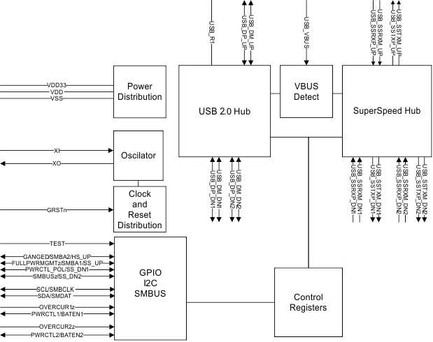
- 8.2 Functional Block Diagram
- 8.3 Feature Description
- 8.4 Device Functional Modes
- 8.5
Register Maps
- 8.5.1
Configuration Registers
- 8.5.1.1 ROM Signature Register
- 8.5.1.2 Vendor ID LSB Register
- 8.5.1.3 Vendor ID MSB Register
- 8.5.1.4 Product ID LSB Register
- 8.5.1.5 Product ID MSB Register
- 8.5.1.6 Device Configuration Register
- 8.5.1.7 Battery Charging Support Register
- 8.5.1.8 Device Removable Configuration Register
- 8.5.1.9 Port Used Configuration Register
- 8.5.1.10 PHY Custom Configuration Register
- 8.5.1.11 Device Configuration Register 2
- 8.5.1.12 UUID Registers
- 8.5.1.13 Language ID LSB Register
- 8.5.1.14 Language ID MSB Register
- 8.5.1.15 Serial Number String Length Register
- 8.5.1.16 Manufacturer String Length Register
- 8.5.1.17 Product String Length Register
- 8.5.1.18 Serial Number Registers
- 8.5.1.19 Manufacturer String Registers
- 8.5.1.20 Product String Registers
- 8.5.1.21 Additional Feature Configuration Register
- 8.5.1.22 Charging Port Control Register
- 8.5.1.23 Device Status and Command Register
- 8.5.1
Configuration Registers
- 9 Applications and Implementation
- 10Power Supply Recommendations
- 11Layout
- 12Device and Documentation Support
- 13Mechanical, Packaging, and Orderable Information
8 Detailed Description
8.1 Overview
The TUSB8020B-Q1 is a two-port USB 3.0 compliant hub. It provides simultaneous SuperSpeed USB and high-speed/full-speed connections on the upstream port and provides SuperSpeed USB, high-speed, full-speed, or low-speed connections on the downstream ports. When the upstream port is connected to an electrical environment that only supports high-speed or full-speed/low-speed connections, SuperSpeed USB connectivity is disabled on the downstream ports. When the upstream port is connected to an electrical environment that only supports full-speed/low-speed connections, SuperSpeed USB and high-speed connectivity are disabled on the downstream ports.
8.2 Functional Block Diagram
8.3 Feature Description
8.3.1 Battery Charging Features
The TUSB8020B-Q1 provides support for USB Battery Charging Specification Revision 1.2 (BC 1.2). Battery charging support may be enabled on a per port basis through the REG_6h(batEn[1:0]).
Battery charging support includes both Charging Downstream Port (CDP) and Dedicated Charging Port (DCP) modes. The DCP mode is compliant with the Chinese Telecommunications Industry Standard YD/T 1591-2009.
In addition, to standard BC 1.2 DCP mode, the TUSB8020B-Q1 provides a mode (AUTOMODE) which automatically provides support for BC 1.2 DCP devices and devices that support custom charging indication. AUTOMODE is enabled by default. When in AUTOMODE, the port will automatically switch between a divider mode and the DCP mode depending on the portable device connected. The divided mode places a fixed DC voltage on the ports DP and DM signals which allows some devices to identify the capabilities of the charger. The default divider mode indicates support for up to 5W. The divider mode can be configured to report a high-current setting (up to 10 W) through REG_Ah(HiCurAcpModeEn).
The battery charging mode for each port is dependent on the state of Reg_6h(batEn[n]), the status of the VBUS input, and the state of REG_Ah(autoModeEnz) upstream port as identified in Table 1. Battery charging can also be enabled through the PWRCTL1/BATEN1 and PWRCTL2/BATEN2 pins.
Table 1. TUSB8020B-Q1 Battery Charging Modes
| batEn[n] | VBUS | autoModeEnz | BC Mode Port x (x = n + 1) |
|---|---|---|---|
| 0 | Don’t Care | Don’t Care | Don’t Care |
| 1 | < 4 V | 0 | Automode(3)(4) |
| 1 | DCP(1)(2) | ||
| > 4 V | Don’t Care | CDP(1) |
8.3.2 USB Power Management
The TUSB8020B-Q1 can be configured for power switched applications using either per-port or ganged power-enable controls and over-current status inputs.
Power switch support is enabled by REG_5h(fullPwrMgmtz) and the per-port or ganged mode is configured by REG_5h(ganged). It can also be enabled through the FULLPWRMGMTz pin. Also ganged or individual control can be controlled by the GANGED pin.
The TUSB8020B-Q1 supports both active high and active low power-enable controls. The PWRCTL[2:1] polarity is configured by REG_Ah(pwrctlPol). The polarity can also be configured by the PWRCTL_POL pin.
8.3.3 One Time Programmable (OTP) Configuration
The TUSB8020B-Q1 allows device configuration through one time programmable non-volatile memory (OTP). The programming of the OTP is supported using vendor-defined USB device requests. For details using the OTP features please contact your TI representative.
Table 2 provides a list features which may be configured using the OTP. The Bit Field section in table shows which features can be controlled by OTP ROM. The bits not listed in the table are not accessible by the OTP ROM.
Table 2. OTP Configurable Features
| CONFIGURATION REGISTER OFFSET | BIT FIELD | DESCRIPTION |
|---|---|---|
| REG_01h | [7:0] | Vendor ID LSB |
| REG_02h | [7:0] | Vendor ID MSB |
| REG_03h | [7:0] | Product ID LSB |
| REG_04h | [7:0] | Product ID MSB |
| REG_07h | [0] | Port removable configuration for downstream ports 1. OTP configuration is inverse of rmbl[1:0], i.e. 1 = not removable, 0 = removable. |
| REG_07h | [1] | Port removable configuration for downstream ports 2. OTP configuration is inverse of rmbl[1:0], i.e. 1 = not removable, 0 = removable. |
| REG_0Ah | [1] | Automode enable |
| REG_0Ah | [4] | High-current divider mode enable. |
| REG_F2h | [3:1] | USB power switch power-on delay. |
8.3.4 Clock Generation
The TUSB8020B-Q1 accepts a crystal input to drive an internal oscillator or an external clock source. If a crystal is used, a 1-MΩ shunt resistor is required. It is also important to keep the XI and XO traces as short as possible and away from any switching leads to minimize noise coupling.
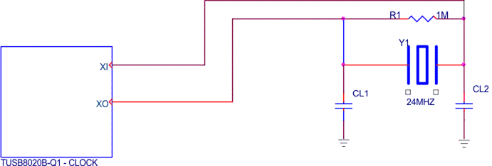 Figure 2. TUSB8020B-Q1 Clock
8.3.4.1 Crystal Requirements
The crystal must be fundamental mode with load capacitance of 12 pF - 24 pF and frequency stability rating of ±100 PPM or better. To ensure proper startup oscillation condition, a maximum crystal equivalent series resistance (ESR) of 50 Ω is recommended. A parallel load capacitor should be used if a crystal source is used. The exact load capacitance value used depends on the crystal vendor. Refer to application note Selection and Specification of Crystals for Texas Instruments USB 2.0 Devices (SLLA122) for details on how to determine the load capacitance value.
8.3.4.2 Input Clock Requirements
When using an external clock source such as an oscillator, the reference clock should have a ±100 PPM or better frequency stability and have less than 50-ps absolute peak to peak jitter or less than 25-ps peak to peak jitter after applying the USB 3.0 jitter transfer function. XI should be tied to the 1.8-V clock source and XO should be left floating.
8.3.5 Power Up and Reset
The TUSB8020B-Q1 does not have specific power sequencing requirements with respect to the VDD or VDD33 power rails. The VDD or VDD33 power rails may be powered up for an indefinite period of time while the other is not powered up if all of these constraints are met:
- All maximum ratings and recommended operating conditions are observed.
- All warnings about exposure to maximum rated and recommended conditions are observed, particularly junction temperature. These apply to power transitions as well as normal operation.
- Bus contention while VDD33 is powered up must be limited to 100 hours over the projected life-time of the device.
- Bus contention while VDD33 is powered down may violate the absolute maximum ratings.
A supply bus is powered up when the voltage is within the recommended operating range. It is powered down when it is below that range, either stable or in transition.
A minimum reset duration of 3 ms is required. This is defined as the time when the power supplies are in the recommended operating range to the de-assertion of GRSTz. This can be generated using programmable-delay supervisory device or using an RC circuit.
8.4 Device Functional Modes
8.4.1 External Configuration Interface
The TUSB8020B-Q1 supports a serial interface for configuration register access. The device may be configured by an attached I2C EEPROM or accessed as a slave by an SMBus capable host controller. The external interface is enabled when both the SCL/SMBCLK and SDA/SMBDAT terminals are pulled up to 3.3 V at the de-assertion of reset. The mode, I2C master or SMBus slave, is determined by the state of SMBUSz/SS_DN2 terminal at reset.
8.4.2 I2C EEPROM Operation
The TUSB8020B-Q1 supports a single-master, standard mode (100 kbit/s) connection to a dedicated I2C EEPROM when the I2C interface mode is enabled. In I2C mode, the TUSB8020B-Q1 reads the contents of the EEPROM at bus address 1010000b using 7-bit addressing starting at address 0.
If the value of the EEPROM contents at byte 00h equals 55h, the TUSB8020B-Q1 loads the configuration registers according to the EEPROM map. If the first byte is not 55h, the TUSB8020B-Q1 exits the I2C mode and continues execution with the default values in the configuration registers. The hub will not connect on the upstream port until the configuration is completed. If the TUSB8020B-Q1 detected an un-programmed EEPROM (value other than 55h), it will enter Programming Mode and a Programming Endpoint within the hub will be enabled.
Note, the bytes located above offset Ah are optional. The requirement for data in those addresses is dependent on the options configured in the Device Configuration, Phy Custom Configuration, and Device Configuration 2 registers.
For details on I2C operation refer to the UM10204 I2C-bus Specification and User Manual.
8.4.3 SMBus Slave Operation
When the SMBus interface mode is enabled, the TUSB8020B-Q1 supports read block and write block protocols as a slave-only SMBus device.
The TUSB8020B-Q1 slave address is 1000 1xyz, where:
- x is the state of GANGED/SMBA2/HS_UP terminal at reset,
- y is the state of FULLPWRMGMTz/SMBA1/SS_UP terminal at reset, and
- z is the read/write bit; 1 = read access, 0 = write access.
If the TUSB8020B-Q1 is addressed by a host using an unsupported protocol it will not respond. The TUSB8020B-Q1 will wait indefinitely for configuration by the SMBus host and will not connect on the upstream port until the SMBus host indicates configuration is complete by clearing the CFG_ACTIVE bit.
For details on SMBus requirements refer to the System Management Bus Specification.
8.5 Register Maps
8.5.1 Configuration Registers
The internal configuration registers are accessed on byte boundaries. The configuration register values are loaded with defaults but can be over-written when the TUSB8020B-Q1 is in I2C or SMBus mode.
Table 3. TUSB8020B-Q1 Register Map
| BYTE ADDRESS | CONTENTS | EEPROM CONFIGURABLE |
|---|---|---|
| 00h | ROM Signature Register | No |
| 01h | Vendor ID LSB | Yes |
| 02h | Vendor ID MSB | Yes |
| 03h | Product ID LSB | Yes |
| 04h | Product ID MSB | Yes |
| 05h | Device Configuration Register | Yes |
| 06h | Battery Charging Support Register | Yes |
| 07h | Device Removable Configuration Register | Yes |
| 08h | Port Used Configuration Register | Yes |
| 09h | Reserved | Yes, program to 00h |
| 0Ah | Device Configuration Register 2 | Yes |
| 0Bh-0Fh | Reserved | |
| 10h-1Fh | UUID Byte [15:0] | No |
| 20h-21h | LangID Byte [1:0] | Yes, if customStrings is set |
| 22h | Serial Number String Length | Yes, if customSerNum is set |
| 23h | Manufacturer String Length | Yes, if customStrings is set |
| 24h | Product String Length | Yes, if customStrings is set |
| 25h-2Fh | Reserved | Yes |
| 30h-4Fh | Serial Number String Byte [31:0] | Yes, if customSerNum is set |
| 50h-8Fh | Manufacturer String Byte [63:0] | Yes, if customStrings is set |
| 90h-CFh | Product String Byte [63:0] | Yes, if customStrings is set |
| D0-DFh | Reserved | No |
| F0h | Additional Feature Configuration Register | Yes |
| F1h | Reserved | No |
| F2h | Charging Port Control Register | Yes |
| F3-F7h | Reserved | No |
| F8h | Device Status and Command Register | No |
| F9-FFh | Reserved | No |
8.5.1.1 ROM Signature Register
Table 4. Register Offset 0h
| Bit No. | 7 | 6 | 5 | 4 | 3 | 2 | 1 | 0 |
| Reset State | 0 | 0 | 0 | 0 | 0 | 0 | 0 | 0 |
Table 5. Bit Descriptions – ROM Signature Register
| Bit | Field Name | Access | Description |
|---|---|---|---|
| 7:0 | romSignature | RW | ROM Signature Register. This register is used by the TUSB8020B-Q1 in I2C mode to validate the attached EEPROM has been programmed. The first byte of the EEPROM is compared to the mask 55h and if not a match, the TUSB8020B-Q1 aborts the EEPROM load and executes with the register defaults. |
8.5.1.2 Vendor ID LSB Register
Table 6. Register Offset 1h
| Bit No. | 7 | 6 | 5 | 4 | 3 | 2 | 1 | 0 |
| Reset State | 0 | 1 | 0 | 1 | 0 | 0 | 0 | 1 |
Table 7. Bit Descriptions – Vendor ID LSB Register
| Bit | Field Name | Access | Description |
|---|---|---|---|
| 7:0 | vendorIdLsb | RO/RW | Vendor ID LSB. Least significant byte of the unique vendor ID assigned by the USB-IF; the default value of this register is 51h representing the LSB of the TI Vendor ID 0451h. The value may be over-written to indicate a customer Vendor ID. This field is read/write unless the OTP ROM VID and OTP ROM PID values are non-zero. If both values are non-zero the value when reading this register shall reflect the OTP ROM value. |
8.5.1.3 Vendor ID MSB Register
Table 8. Register Offset 2h
| Bit No. | 7 | 6 | 5 | 4 | 3 | 2 | 1 | 0 |
| Reset State | 0 | 0 | 0 | 0 | 0 | 1 | 0 | 0 |
Table 9. Bit Descriptions – Vendor ID MSB Register
| Bit | Field Name | Access | Description |
|---|---|---|---|
| 7:0 | vendorIdMsb | RO/RW | Vendor ID MSB. Most significant byte of the unique vendor ID assigned by the USB-IF; the default value of this register is 04h representing the MSB of the TI Vendor ID 0451h. The value may be over-written to indicate a customer Vendor ID. This field is read/write unless the OTP ROM VID and OTP ROM PID values are non-zero. If both values are non-zero the value when reading this register shall reflect the OTP ROM value. |
8.5.1.4 Product ID LSB Register
Table 10. Register Offset 3h
| Bit No. | 7 | 6 | 5 | 4 | 3 | 2 | 1 | 0 |
| Reset State | 0 | 0 | 1 | 0 | 0 | 1 | 0 | 1 |
Table 11. Bit Descriptions – Product ID LSB Register
| Bit | Field Name | Access | Description |
|---|---|---|---|
| 7:0 | productIdLsb | RO/RW | Product ID LSB. Least significant byte of the product ID assigned by Texas Instruments and reported in the SuperSpeed Device descriptor. The default value of this register is 25h representing the LSB of the SuperSpeed product ID assigned by Texas Instruments. The value reported in the USB 2.0 Device descriptor is the value of this register bit wise XORed with 00000010b. The value may be over-written to indicate a customer product ID. This field is read/write unless the OTP ROM VID and OTP ROM PID values are non-zero. If both values are non-zero the value when reading this register shall reflect the OTP ROM value. |
8.5.1.5 Product ID MSB Register
Table 12. Register Offset 4h
| Bit No. | 7 | 6 | 5 | 4 | 3 | 2 | 1 | 0 |
| Reset State | 1 | 0 | 0 | 0 | 0 | 0 | 0 | 0 |
Table 13. Bit Descriptions – Product ID MSB Register
| Bit | Field Name | Access | Description |
|---|---|---|---|
| 7:0 | productIdMsb | RO/RW | Product ID MSB. Most significant byte of the product ID assigned by Texas Instruments; the default value of this register is 80h representing the MSB of the product ID assigned by Texas Instruments. The value may be over-written to indicate a customer product ID. This field is read/write unless the OTP ROM VID and OTP ROM PID values are non-zero. If both values are non-zero, the value when reading this register will reflect the OTP ROM value. |
8.5.1.6 Device Configuration Register
Table 14. Register Offset 5h
| Bit No. | 7 | 6 | 5 | 4 | 3 | 2 | 1 | 0 |
| Reset State | 0 | 0 | 0 | 1 | X | X | 0 | 0 |
Table 15. Bit Descriptions – Device Configuration Register
| Bit | Field Name | Access | Description | |
|---|---|---|---|---|
| 7 | customStrings | RW | Custom strings enable. This bit controls the ability to write to the Manufacturer String Length, Manufacturer String, Product String Length, Product String, and Language ID registers | |
| 0 = The Manufacturer String Length, Manufacturer String, Product String Length, Product String, and Language ID registers are read only | ||||
| 1 = The Manufacturer String Length, Manufacturer String, Product String Length, Product String, and Language ID registers may be loaded by EEPROM or written by SMBus | ||||
| The default value of this bit is 0. | ||||
| 6 | customSernum | RW | Custom serial number enable. This bit controls the ability to write to the serial number registers. | |
| 0 = The Serial Number String Length and Serial Number String registers are read only | ||||
| 1 = The Serial Number String Length and Serial Number String registers may be loaded by EEPROM or written by SMBus | ||||
| The default value of this bit is 0. | ||||
| 5 | u1u2Disable | RW | U1 U2 Disable. This bit controls the U1/U2 support. | |
| 0 = U1/U2 support is enabled | ||||
| 1 = U1/U2 support is disabled, the TUSB8020B-Q1 will not initiate or accept any U1 or U2 requests on any port, upstream or downstream, unless it receives or sends a Force_LinkPM_Accept LMP. After receiving or sending an FLPMA LMP, it will continue to enable U1 and U2 according to USB 3.0 protocol until it gets a power-on reset or is disconnected on its upstream port. | ||||
| When the TUSB8020B-Q1 is in I2C mode, the TUSB8020B-Q1 loads this bit from the contents of the EEPROM. | ||||
| When the TUSB8020B-Q1 is in SMBUS mode, the value may be over-written by an SMBus host. | ||||
| 4 | RSVD | RO | Reserved. This bit is reserved and returns 1 when read. | |
| 3 | ganged | RW | Ganged. This bit is loaded at the de-assertion of reset with the value of the GANGED/SMBA2/HS_UP terminal. | |
| 0 = When fullPwrMgmtz = 0, each port is individually power switched and enabled by the PWRCTL[2:1]/BATEN[2:1] terminals | ||||
| 1 = When fullPwrMgmtz = 0, the power switch control for all ports is ganged and enabled by the PWRCTL1/BATEN1 terminal | ||||
| When the TUSB8020B-Q1 is in I2C mode, the TUSB8020B-Q1 loads this bit from the contents of the EEPROM. | ||||
| When the TUSB8020B-Q1 is in SMBUS mode, the value may be over-written by an SMBus host. | ||||
| 2 | fullPwrMgmtz | RW | Full Power Management. This bit is loaded at the de-assertion of reset with the value of the FULLPWRMGMTz/SMBA1/SS_UP terminal. | |
| 0 = Port power switching and over-current status reporting is enabled | ||||
| 1 = Port power switching and over-current status reporting is disabled | ||||
| When the TUSB8020B-Q1 is in I2C mode, the TUSB8020B-Q1 loads this bit from the contents of the EEPROM. | ||||
| When the TUSB8020B-Q1 is in SMBUS mode, the value may be over-written by an SMBus host. | ||||
| 1 | RSVD | RW | Reserved. This bit is reserved and should not be altered from the default. | |
| 0 | RSVD | RO | Reserved. This field is reserved and returns 0 when read. | |
8.5.1.7 Battery Charging Support Register
Table 16. Register Offset 6h
| Bit No. | 7 | 6 | 5 | 4 | 3 | 2 | 1 | 0 |
| Reset State | 0 | 0 | 0 | 0 | 0 | 0 | X | X |
Table 17. Bit Descriptions – Battery Charging Support Register
| Bit | Field Name | Access | Description | |
|---|---|---|---|---|
| 7:2 | RSVD | RO | Reserved. Read only, returns 0 when read. | |
| 1:0 | batEn[1:0] | RW | Battery Charger Support. The bits in this field indicate whether the downstream port implements the charging port features. | |
| 0 = The port is not enabled for battery charging support features | ||||
| 1 = The port is enabled for battery charging support features | ||||
| Each bit corresponds directly to a downstream port, i.e. batEn0 corresponds to downstream port 1, and batEN1 corresponds to downstream port 2. | ||||
| The default value for these bits are loaded at the de-assertion of reset with the value of PWRCTL/BATEN[1:0]. | ||||
| When in I2C/SMBus mode the bits in this field may be over-written by EEPROM contents or by an SMBus host. | ||||
8.5.1.8 Device Removable Configuration Register
Table 18. Register Offset 7h
| Bit No. | 7 | 6 | 5 | 4 | 3 | 2 | 1 | 0 |
| Reset State | 0 | 0 | 0 | 0 | 0 | 0 | X | X |
Table 19. Bit Descriptions – Device Removable Configuration Register
| Bit | Field Name | Access | Description | |
|---|---|---|---|---|
| 7 | customRmbl | RW | Custom removable status. When this field is a 1, the TUSB8020B-Q1 uses rmbl bits in this register to identify removable status for the ports. | |
| 6:2 | RSVD | RO | Reserved. Read only, returns 0 when read. Bits 3:2 are RW. They are reserved and return zero when read. | |
| 1:0 | rmbl[1:0] | RW | Removable. The bits in this field indicate whether a device attached to downstream ports 2 through 1 are removable or permanently attached. | |
| 0 = The device attached to the port is not removable | ||||
| 1 = The device attached to the port is removable | ||||
| Each bit corresponds directly to a downstream port n + 1, i.e. rmbl0 corresponds to downstream port 1, rmbl1 corresponds to downstream port 2, etc. | ||||
| This field is read only unless the customRmbl bit is set to 1. Otherwise the value of this filed reflects the inverted values of the OTP ROM non_rmb[1:0] field. | ||||
8.5.1.9 Port Used Configuration Register
Table 20. Register Offset 8h
| Bit No. | 7 | 6 | 5 | 4 | 3 | 2 | 1 | 0 |
| Reset State | 0 | 0 | 0 | 0 | 0 | 0 | 1 | 1 |
Table 21. Bit Descriptions – Port Used Configuration Register
| Bit | Field Name | Access | Description |
|---|---|---|---|
| 7:0 | RSVD | RO | Reserved. Read only. |
8.5.1.10 PHY Custom Configuration Register
Table 22. Register Offset 9h
| Bit No. | 7 | 6 | 5 | 4 | 3 | 2 | 1 | 0 |
| Reset State | 0 | 0 | 0 | 0 | 0 | 0 | 0 | 0 |
Table 23. Bit Descriptions – PHY Custom Configuration Register
| Bit | Field Name | Access | Description |
|---|---|---|---|
| 7:6 | RSVD | RO | Reserved. Read only, returns 0 when read. |
| 5 | RSVD | RW | Reserved. This bit is reserved and should not be altered from the default. |
| 4:2 | RSVD | RO | Reserved. Read only, returns 0 when read. |
| 1:0 | RSVD | RW | Reserved. This field is reserved and should not be altered from the default. |
8.5.1.11 Device Configuration Register 2
Table 24. Register Offset Ah
| Bit No. | 7 | 6 | 5 | 4 | 3 | 2 | 1 | 0 |
| Reset State | 0 | 0 | X | 0 | 0 | 0 | 0 | 0 |
Table 25. Bit Descriptions – Device Configuration Register 2
| Bit | Field Name | Access | Description | |
|---|---|---|---|---|
| 7 | RSVD | RO | Reserved. Read only, returns 0 when read. | |
| 6 | customBCfeatures | RW | Custom Battery Charging Feature Enable. This bit controls the ability to write to the battery charging feature configuration controls. | |
| 0 = The HiCurAcpModeEn and AutoModeEnz bits are read only and the values are loaded from the OTP ROM. | ||||
| 1 = The HiCurAcpModeEn and AutoModeEnz bits are read/write and can be loaded by EEPROM or written by SMBus. from this register. | ||||
| This bit may be written simultaneously with HiCurAcpModeEn and AutoModeEnz. | ||||
| 5 | pwrctlPol | RW | Power enable polarity. This bit is loaded at the de-assertion of reset with the inverse value of the PWRCTL_POL terminal. | |
| 0 = PWRCTL polarity is active low | ||||
| 1 = PWRCTL polarity is active high | ||||
| When the TUSB8020B-Q1 is in I2C mode, the TUSB8020B-Q1 loads this bit from the contents of the EEPROM. | ||||
| When the TUSB8020B-Q1 is in SMBUS mode, the value may be over-written by an SMBus host. | ||||
| 4 | HiCurAcpModeEn | RO/RW | High-current ACP mode enable. This bit enables the high-current tablet charging mode when the automatic battery charging mode is enabled for downstream ports. | |
| 0 = High current divider mode disabled | ||||
| 1 = High current divider mode enabled | ||||
| This bit is read only unless the customBCfeatures bit is set to 1. Otherwise the value of this bit reflects the value of the OTP ROM HiCurAcpModeEn bit. | ||||
| 3 | RSVD | RW | Reserved | |
| 2 | dsportEcrEn | RW | DSPort ECR enable. This bit enables full implementation of the DSPORT ECR (April 2013). | |
| 0 = DSPort ECR (April 2013) is enabled with the exception of changes related to the CCS bit is set upon entering U0, and changes related to avoiding or reporting compliance mode entry. | ||||
| 1 = The full DSport ECR (April 2013) is enabled. | ||||
| 1 | autoModeEnz | RO/RW | Automatic Mode Enable. This bit is loaded from the OTP ROM. | |
| The automatic mode only applies to downstream ports with battery charging enabled when the upstream port is not connected. Under these conditions: | ||||
| 0 = Automatic mode battery charging features are enabled. | ||||
| 1 = Automatic mode is disabled; only Battery Charging 1.2 DCP mode is supported. | ||||
| NOTE: When the upstream port is connected, Battery Charging 1.2 CDP mode will be supported on all ports that enabled for battery charging support regardless of the value of this bit. The Automode is enabled if this field is zero and the pwrctlPol field is zero. | ||||
| This bit is read only unless the customBCfeatures bit is set to 1. Otherwise the value of this bit reflects the value of the OTP ROM AutoModeEnz bit. | ||||
| 0 | RSVD | RO | Reserved. Read only, returns 0 when read. | |
8.5.1.12 UUID Registers
Table 26. Register Offset 10h-1Fh
| Bit No. | 7 | 6 | 5 | 4 | 3 | 2 | 1 | 0 |
| Reset State | X | X | X | X | X | X | X | X |
Table 27. Bit Descriptions – UUID Byte N Register
| Bit | Field Name | Access | Description |
|---|---|---|---|
| 7:0 | uuidByte[n] | RO | UUID byte N. The UUID returned in the Container ID descriptor. The value of this register is provided by the device and is meets the UUID requirements of Internet Engineering Task Force (IETF) RFC 4122 A UUID URN Namespace. |
8.5.1.13 Language ID LSB Register
Table 28. Register Offset 20h
| Bit No. | 7 | 6 | 5 | 4 | 3 | 2 | 1 | 0 |
| Reset State | 0 | 0 | 0 | 0 | 1 | 0 | 0 | 1 |
Table 29. Bit Descriptions – Language ID LSB Register
| Bit | Field Name | Access | Description |
|---|---|---|---|
| 7:0 | langIdLsb | RW | Language ID least significant byte. This register contains the value returned in the LSB of the LANGID code in string index 0. The TUSB8020B-Q1 only supports one language ID. The default value of this register is 09h representing the LSB of the LangID 0409h indicating English United States. When customStrings is 1, this field may be over-written by the contents of an attached EEPROM or by an SMBus host. |
8.5.1.14 Language ID MSB Register
Table 30. Register Offset 21h
| Bit No. | 7 | 6 | 5 | 4 | 3 | 2 | 1 | 0 |
| Reset State | 0 | 0 | 0 | 0 | 0 | 1 | 0 | 0 |
Table 31. Bit Descriptions – Language ID MSB Register
| Bit | Field Name | Access | Description |
|---|---|---|---|
| 7:0 | langIdMsb | RO/RW | Language ID most significant byte. This register contains the value returned in the MSB of the LANGID code in string index 0. The TUSB8020B-Q1 only supports one language ID. The default value of this register is 04h representing the MSB of the LangID 0409h indicating English United States. When customStrings is 1, this field may be over-written by the contents of an attached EEPROM or by an SMBus host. |
8.5.1.15 Serial Number String Length Register
Table 32. Register Offset 22h
| Bit No. | 7 | 6 | 5 | 4 | 3 | 2 | 1 | 0 |
| Reset State | 0 | 0 | 0 | 1 | 1 | 0 | 0 | 0 |
Table 33. Bit Descriptions – Serial Number String Length Register
| Bit | Field Name | Access | Description |
|---|---|---|---|
| 7:6 | RSVD | RO | Reserved. Read only, returns 0 when read. |
| 5:0 | serNumStringLen | RO/RW | Serial number string length. The string length in bytes for the serial number string. The default value is 18h indicating that a 24 byte serial number string is supported. The maximum string length is 32 bytes. When customSernum is 1, this field may be over-written by the contents of an attached EEPROM or by an SMBus host. When the field is non-zero, a serial number string of serNumbStringLen bytes is returned at string index 1 from the data contained in the Serial Number String registers. |
8.5.1.16 Manufacturer String Length Register
Table 34. Register Offset 23h
| Bit No. | 7 | 6 | 5 | 4 | 3 | 2 | 1 | 0 |
| Reset State | 0 | 0 | 0 | 0 | 0 | 0 | 0 | 0 |
Table 35. Bit Descriptions – Manufacturer String Length Register
| Bit | Field Name | Access | Description |
|---|---|---|---|
| 7 | RSVD | RO | Reserved. Read only, returns 0 when read. |
| 6:0 | mfgStringLen | RO/RW | Manufacturer string length. The string length in bytes for the manufacturer string. The default value is 0, indicating that a manufacturer string is not provided. The maximum string length is 64 bytes. When customStrings is 1, this field may be over-written by the contents of an attached EEPROM or by an SMBus host. When the field is non-zero, a manufacturer string of mfgStringLen bytes is returned at string index 3 from the data contained in the Manufacturer String registers. |
8.5.1.17 Product String Length Register
Table 36. Register Offset 24h
| Bit No. | 7 | 6 | 5 | 4 | 3 | 2 | 1 | 0 |
| Reset State | 0 | 0 | 0 | 0 | 0 | 0 | 0 | 0 |
Table 37. Bit Descriptions – Product String Length Register
| Bit | Field Name | Access | Description |
|---|---|---|---|
| 7 | RSVD | RO | Reserved. Read only, returns 0 when read. |
| 6:0 | prodStringLen | RO/RW | Product string length. The string length in bytes for the product string. The default value is 0, indicating that a product string is not provided. The maximum string length is 64 bytes. When customStrings is 1, this field may be over-written by the contents of an attached EEPROM or by an SMBus host. When the field is non-zero, a product string of prodStringLen bytes is returned at string index 2 from the data contained in the Product String registers. |
8.5.1.18 Serial Number Registers
Table 38. Register Offset 30h-4Fh
| Bit No. | 7 | 6 | 5 | 4 | 3 | 2 | 1 | 0 |
| Reset State | X | X | x | x | x | x | x | x |
Table 39. Bit Descriptions – Serial Number Registers
| Bit | Field Name | Access | Description |
|---|---|---|---|
| 7:0 | serialNumber[n] | RO/RW | Serial Number byte N. The serial number returned in the Serial Number string descriptor at string index 1. The default value of these registers is set by TI. When customSernum is 1, these registers may be over-written by EEPROM contents or by an SMBus host. |
8.5.1.19 Manufacturer String Registers
Table 40. Register Offset 50h-8Fh
| Bit No. | 7 | 6 | 5 | 4 | 3 | 2 | 1 | 0 |
| Reset State | 0 | 0 | 0 | 0 | 0 | 0 | 0 | 0 |
Table 41. Bit Descriptions – Manufacturer String Registers
| Bit | Field Name | Access | Description |
|---|---|---|---|
| 7:0 | mfgStringByte[n] | RO/RW | Manufacturer string byte N. These registers provide the string values returned for string index 3 when mfgStringLen is greater than 0. The number of bytes returned in the string is equal to mfgStringLen. The programmed data should be in UNICODE UTF-16LE encodings as defined by The Unicode Standard, Worldwide Character Encoding, Version 5.0. |
8.5.1.20 Product String Registers
Table 42. Register Offset 90h-CFh
| Bit No. | 7 | 6 | 5 | 4 | 3 | 2 | 1 | 0 |
| Reset State | 0 | 0 | 0 | 0 | 0 | 0 | 0 | 0 |
Table 43. Bit Descriptions – Product String Byte N Register
| Bit | Field Name | Access | Description |
|---|---|---|---|
| 7:0 | prodStringByte[n] | RW | Product string byte N. These registers provide the string values returned for string index 2 when prodStringLen is greater than 0. The number of bytes returned in the string is equal to prodStringLen. The programmed data should be in UNICODE UTF-16LE encodings as defined by The Unicode Standard, Worldwide Character Encoding, Version 5.0. |
8.5.1.21 Additional Feature Configuration Register
Table 44. Register Offset F0h
| Bit No. | 7 | 6 | 5 | 4 | 3 | 2 | 1 | 0 |
| Reset State | 0 | 0 | 0 | 0 | 0 | 0 | 0 | 0 |
Table 45. Bit Descriptions – Additional Feature Configuration Register
| Bit | Field Name | Access | Description | |
|---|---|---|---|---|
| 7:1 | RSVD | RO | Reserved. Read only, returns 0 when read. | |
| 0 | usb3spreadDis | RW | USB3 Spread Spectrum Disable. This bit allows firmware to disable the spread spectrum function of the USB3 phy PLL. | |
| 0 = Spread spectrum function is enabled | ||||
| 1= Spread spectrum function is disabled | ||||
| This bit is loaded at the de-assertion of reset with the value of the SCL/SMBCLK terminal. | ||||
8.5.1.22 Charging Port Control Register
Table 46. Register Offset F2h
| Bit No. | 7 | 6 | 5 | 4 | 3 | 2 | 1 | 0 |
| Reset State | 0 | 0 | 0 | 0 | 0 | 0 | 0 | 0 |
Table 47. Bit Descriptions – Charging Port Control Register
| Bit | Field Name | Access | Description |
|---|---|---|---|
| 7:4 | RSVD | RO | Reserved. Read only, returns 0 when read. |
| 3:1 | pwronTime | RW | Power On Delay Time. When dsportEcrEn is set, this field sets the delay time from the removal disable of PWRCTL to the enable of PWRCTL when transitioning battery charging modes. For example, when disabling the power on a transition from custom charging mode to Dedicated Charging Port Mode. The nominal timing is defined as follows:
Equation 1. TPWRON_EN = (pwronTime + 1) x 200 ms
These registers may be over-written by EEPROM contents or by an SMBus host. |
| 0 | RSVD | RW | Reserved. This bit is reserved and should not be altered from the default. |
8.5.1.23 Device Status and Command Register
Table 48. Register Offset F8h
| Bit No. | 7 | 6 | 5 | 4 | 3 | 2 | 1 | 0 |
| Reset State | 0 | 0 | 0 | 0 | 0 | 0 | 0 | 0 |
Table 49. Bit Descriptions – Device Status and Command Register
| Bit | Field Name | Access | Description |
|---|---|---|---|
| 7:2 | RSVD | RO | Reserved. Read only, returns 0 when read. |
| 1 | smbusRst | RSU | SMBus interface reset. This bit loads the registers back to their GRSTz values. This bit is set by writing a 1 and is cleared by hardware on completion of the reset. A write of 0 has no effect. |
| 0 | cfgActive | RCU | Configuration active. This bit indicates that configuration of the TUSB8020B-Q1 is currently active. The bit is set by hardware when the device enters the I2C or SMBus mode. The TUSB8020B-Q1 shall not connect on the upstream port while this bit is 1. When in the SMBus mode, this bit must be cleared by the SMBus host in order to exit the configuration mode and allow the upstream port to connect. The bit is cleared by a writing 1. A write of 0 has no effect. |