SLAZ242O October 2012 – May 2021 MSP430F4784
- 1Functional Advisories
- 2Preprogrammed Software Advisories
- 3Debug Only Advisories
- 4Fixed by Compiler Advisories
- 5Nomenclature, Package Symbolization, and Revision Identification
-
6Advisory Descriptions
- 6.1 COMP3
- 6.2 CPU19
- 6.3 CPU44
- 6.4 EEM20
- 6.5 FLASH19
- 6.6 FLASH24
- 6.7 FLASH25
- 6.8 FLASH27
- 6.9 FLASH36
- 6.10 FLL4
- 6.11 FLL5
- 6.12 FLL6
- 6.13 FLL7
- 6.14 JTAG23
- 6.15 LCDA5
- 6.16 LCDA7
- 6.17 SDA4
- 6.18 TA12
- 6.19 TA16
- 6.20 TA21
- 6.21 TAB22
- 6.22 TB2
- 6.23 TB16
- 6.24 TB24
- 6.25 USCI15
- 6.26 USCI19
- 6.27 USCI20
- 6.28 USCI21
- 6.29 USCI22
- 6.30 USCI23
- 6.31 USCI24
- 6.32 USCI25
- 6.33 USCI26
- 6.34 USCI28
- 6.35 USCI30
- 6.36 USCI34
- 6.37 USCI35
- 6.38 USCI40
- 6.39 XOSC5
- 6.40 XOSC8
- 6.41 XOSC9
- 7Revision History
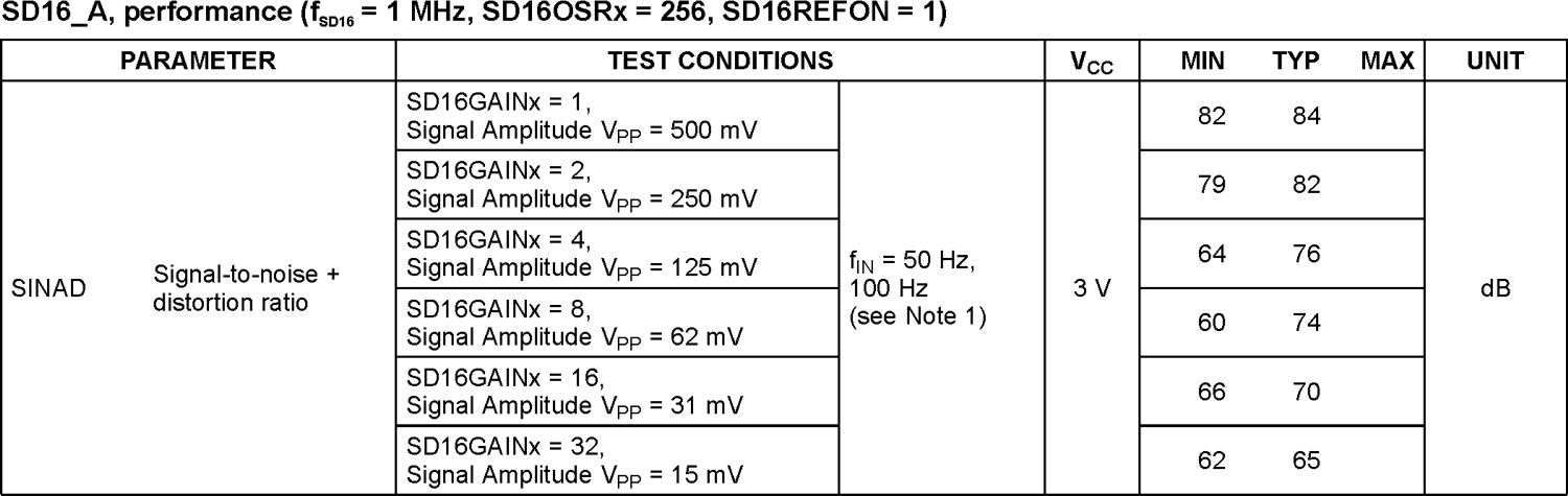
6.17 SDA4
SDA Module
Category
Functional
Function
Reduced SINAD performance at certain input voltage levels
Description
The performance of the SD16_A maybe degraded due to reduced SINAD when the level of the analog input is between 20mV and 120mV. This can occur on any channel, irrespective of their PGA settings.
Workaround
1. Avoid the use of any PGA settings less than 16 with the common-mode voltage of zero, which most likely accommodates input signal levels that fall under this range.
or
2. Introduce a common-mode voltage, such as internal reference voltage of 1.2 V, to ensure that the input signal level is outside the range of 20 mV to 120 mV.
The following table shows the SD16_A performance with common mode voltage of zero: