SLAAE45 September 2021 TMUXHS4412
2.3 Vias, Stub, and ESD/EMI Layout Guidelines
- The use of vias is essential in
most routings, but vias add additional inductance and capacitance, and
reflections occur due to the change in the characteristic impedance. Vias also
increase the trace length.
If possible, avoid routing high-speed traces through the vias.
If it is impossible to avoid vias:
- Ensure that the via count on each member of the differential pair is equal and that the vias are as equally spaced as possible. A maximum of two vias are recommended for high-speed trace over 5Gbps.
- Be careful with the
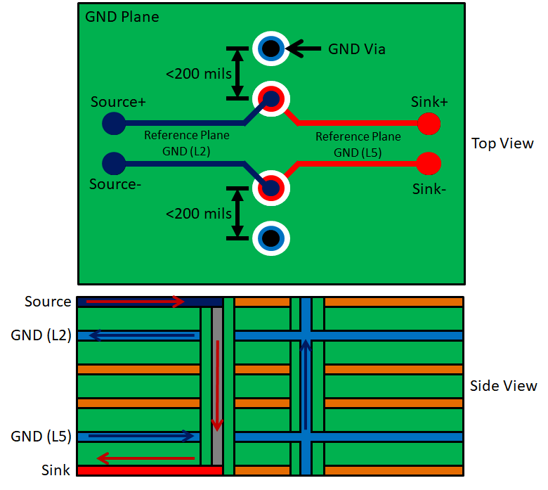
return current when changing the layers. Use ground vias around the
signal via to make sure that the return current can flow as close as
possible to the signal (see Figure 2-3)
 Figure 2-3 Differential
Pair Via Return Path With GND Vias
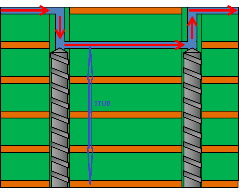
 - Longer via stubs resonate
at lower frequencies and increase insertion loss, keep these stubs as
short as possible. TI recommends keeping via stubs to less than 15 mils.
Longer stubs must be back-drilled (see Figure 2-4).
 Figure 2-4 Long Vias With
Back-Drilled Stubs
- Do not place probe or test points on any high-speed differential signals.
- Do not route high-speed traces under or near crystals, oscillators, clock signal generators, switching power regulators, mounting holes, magnetic devices, or integrated circuits (IC) that use or duplicate clock signals.
- When choosing ESD/EMI
components, TI recommends selecting devices that permit flow-through routing of
the differential signal pair because they provide the cleanest routing.
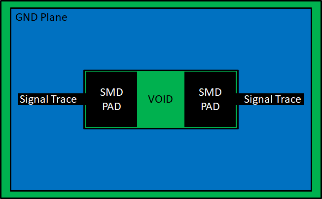
- Incorporate voids under
the ESD/EMI component signal pads to reduce losses (see Figure 2-5).
 Figure 2-5 Void Below
Surface Mount Devices
 - Use 0402 0-Ω resistors for common-mode filter (CMF) no-stuff options because larger components will typically introduce more loss that the CMF itself.
- Keep the overall routing of AC coupling capacitors+ CMF+ ESD protection as short and as close as possible to the connector.
- Incorporate voids under
the ESD/EMI component signal pads to reduce losses (see Figure 2-5).