-
TCA9539 Low Voltage 16-Bit I2C and SMBus Low-Power I/O Expander with Interrupt Output, Reset Pin, and Configuration Registers
- 1 Features
- 2 Applications
- 3 Description
- 4 Revision History
- 5 Pin Configuration and Functions
- 6 Specifications
- 7 Parameter Measurement Information
- 8 Detailed Description
- 9 Application and Implementation
- 10Power Supply Recommendations
- 11Layout
- 12Device and Documentation Support
- 13Mechanical, Packaging, and Orderable Information
- IMPORTANT NOTICE
TCA9539 Low Voltage 16-Bit I2C and SMBus Low-Power I/O Expander with Interrupt Output, Reset Pin, and Configuration Registers
1 Features
- I2C to Parallel Port Expander
- Low Standby-Current Consumption
- Open-Drain Active-Low Interrupt Output
- Active-Low Reset Input
- 5-V Tolerant I/O Ports
- Compatible With Most Microcontrollers
- 400-kHz Fast I2C Bus
- Input and Output Configuration Register
- Polarity Inversion Register
- Internal Power-on Reset
- No Glitch on Power Up
- Noise Filter on SCL and SDA Inputs
- Address by Two Hardware Address Pins for Use of up to Four Devices
- Latched Outputs With High-Current Drive Capability for Directly Driving LEDs
- Latch-Up Performance Exceeds 100 mA Per JESD 78, Class II
- ESD Protection Exceeds JESD 22
- 2000-V Human-Body Model (A114-A)
- 1000-V Charged-Device Model (C101)
2 Applications
- Servers
- Routers (Telecom Switching Equipment)
- Personal Computers, smartphones
- Industrial Automation
- I2C GPIO Expansion
3 Description
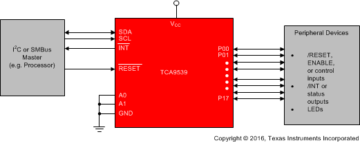
The TCA9539 is a 24-pin device that provides 16 bits of general purpose parallel input and output (I/O) expansion for the two-line bidirectional I2C bus (or SMBus protocol). The device can operate with a power supply voltage (VCC) range from 1.65 V to 5.5 V. The device supports 100-kHz (I2C Standard mode) and 400-kHz (I2C Fast mode) clock frequencies. I/O expanders such as the TCA9539 provide a simple solution when additional I/Os are needed for switches, sensors, push-buttons, LEDs, fans, and other similar devices.
The features of the TCA9539 include an interrupt that is generated on the INT pin whenever an input port changes state. The A0 and A1 hardware selectable address pins allow up to four TCA9539 devices on the same I2C bus. The device can be reset to its default state by cycling the power supply and causing a power-on-reset. Also, the TCA9539 has a hardware RESET pin that can be used to reset the device to its default state.
Device Information(1)
| PART NUMBER | PACKAGE | BODY SIZE (NOM) |
|---|---|---|
| TCA9539 | TSSOP (24) | 7.80 mm × 4.40 mm |
| WQFN (24) | 4.00 mm × 4.00 mm | |
| VQFN (24) | 4.00 mm × 4.00 mm |
- For all available packages, see the orderable addendum at the end of the data sheet.
Simplified Schematic
4 Revision History
Changes from B Revision (October 2015) to C Revision
- Made changes to Interrupt (INT) Output and Reads sectionGo
- Made changes to Recommended Operating ConditionsGo
- Made changes to Electrical CharacteristicsGo
- Added IOL for different Tj Go
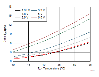
- Removed ΔICC spec from the Electrical Characteristics table, added ΔICC typical characteristics graph Go
- Changed ICC standby into different input states, with increased maximums Go
- Changed Cio maximum Go
- Clarified interrupt reset time (tir) with respect to falling edge of ACK related SCL pulse. Go
- Updated Figure 33 and Figure 34Go
- Power on reset requirements relaxed Go
Changes from A Revision (September 2009) to B Revision
- Added ESD Ratings table, Feature Description section, Device Functional Modes, Application and Implementation section, Power Supply Recommendations section, Layout section, Device and Documentation Support section, and Mechanical, Packaging, and Orderable Information section. Go
- Added RGE package.Go
- Added Thermal Information table Go
- Added "Time to reset; VCC = 1.65 V - 2.3 V" parameter to RESET Timing Requirements table. Go
- Added "Output data valid; VCC = 1.65 V - 2.3 V to Switching Characteristics table. Go
5 Pin Configuration and Functions
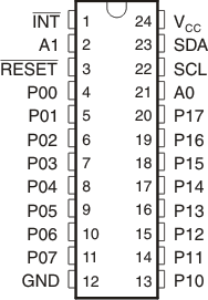
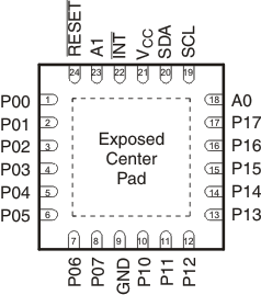
Pin Functions
| NAME | NO. | I/O | DESCRIPTION | |
|---|---|---|---|---|
| TSSOP (PW) |
QFN (RTW, RGE) |
|||
| A0 | 21 | 18 | I | Address input. Connect directly to VCC or ground |
| A1 | 2 | 23 | I | Address input. Connect directly to VCC or ground |
| GND | 12 | 9 | — | Ground |
| INT | 1 | 22 | O | Interrupt open-drain output. Connect to VCC through a pull-up resistor |
| RESET | 3 | 24 | I | Active-low reset input. Connect to VCC through a pull-up resistor if no active connection is used |
| P00 | 4 | 1 | I/O | P-port input-output. Push-pull design structure. At power on, P00 is configured as an input |
| P01 | 5 | 2 | I/O | P-port input-output. Push-pull design structure. At power on, P01 is configured as an input |
| P02 | 6 | 3 | I/O | P-port input-output. Push-pull design structure. At power on, P02 is configured as an input |
| P03 | 7 | 4 | I/O | P-port input-output. Push-pull design structure. At power on, P03 is configured as an input |
| P04 | 8 | 5 | I/O | P-port input-output. Push-pull design structure. At power on, P04 is configured as an input |
| P05 | 9 | 6 | I/O | P-port input-output. Push-pull design structure. At power on, P05 is configured as an input |
| P06 | 10 | 7 | I/O | P-port input-output. Push-pull design structure. At power on, P06 is configured as an input |
| P07 | 11 | 8 | I/O | P-port input-output. Push-pull design structure. At power on, P07 is configured as an input |
| P10 | 13 | 10 | I/O | P-port input-output. Push-pull design structure. At power on, P10 is configured as an input |
| P11 | 14 | 11 | I/O | P-port input-output. Push-pull design structure. At power on, P11 is configured as an input |
| P12 | 15 | 12 | I/O | P-port input-output. Push-pull design structure. At power on, P12 is configured as an input |
| P13 | 16 | 13 | I/O | P-port input-output. Push-pull design structure. At power on, P13 is configured as an input |
| P14 | 17 | 14 | I/O | P-port input-output. Push-pull design structure. At power on, P14 is configured as an input |
| P15 | 18 | 15 | I/O | P-port input-output. Push-pull design structure. At power on, P15 is configured as an input |
| P16 | 19 | 16 | I/O | P-port input-output. Push-pull design structure. At power on, P16 is configured as an input |
| P17 | 20 | 17 | I/O | P-port input-output. Push-pull design structure. At power on, P17 is configured as an input |
| SCL | 22 | 19 | I | Serial clock bus. Connect to VCC through a pull-up resistor |
| SDA | 23 | 20 | I/O | Serial data bus. Connect to VCC through a pull-up resistor |
| VCC | 24 | 21 | — | Supply voltage |
6 Specifications
6.1 Absolute Maximum Ratings
over operating free-air temperature range (unless otherwise noted) (1)| MIN | MAX | UNIT | |||
|---|---|---|---|---|---|
| VCC | Supply voltage | –0.5 | 6 | V | |
| VI | Input voltage(2) | –0.5 | 6 | V | |
| VO | Output voltage (2) | –0.5 | 6 | V | |
| IIK | Input clamp current | VI < 0 | –20 | mA | |
| IOK | Output clamp current | VO < 0 | –20 | mA | |
| IIOK | Input-output clamp current | VO < 0 or VO > VCC | ±20 | mA | |
| IOL | Continuous output low current | VO = 0 to VCC | 50 | mA | |
| IOH | Continuous output high current | VO = 0 to VCC | –50 | mA | |
| ICC | Continuous current through GND | –250 | mA | ||
| Continuous current through VCC | 160 | ||||
| Tj(MAX) | Maximum junction temperature | 100 | °C | ||
| Tstg | Storage temperature | –65 | 150 | °C | |
6.2 ESD Ratings
| VALUE | UNIT | |||
|---|---|---|---|---|
| V(ESD) | Electrostatic discharge | Human-body model (HBM), per ANSI/ESDA/JEDEC JS-001 (1) | ±2000 | V |
| Charged-device model (CDM), per JEDEC specification JESD22-C101 (2) | ±1000 | |||
6.3 Recommended Operating Conditions
| MIN | MAX | UNIT | ||||
|---|---|---|---|---|---|---|
| VCC | Supply voltage | 1.65 | 5.5 | V | ||
| VIH | High-level input voltage | SCL, SDA | 0.7 × VCC | VCC (1) | V | |
| A0, A1, RESET, P07–P00, P10–P17 | 0.7 × VCC | 5.5 | ||||
| VIL | Low-level input voltage | SCL, SDA, A0, A1, RESET, P07–P00, P10–P17 | –0.5 | 0.3 × VCC | V | |
| IOH | High-level output current | P07–P00, P17–P10 | –10 | mA | ||
| IOL | Low-level output current(2) | P00–P07, P10–P17 | Tj ≤ 65°C | 25 | mA | |
| Tj ≤ 85°C | 18 | |||||
| Tj ≤ 100°C | 11 | |||||
| IOL | Low-level output current(2) | INT, SDA | Tj ≤ 85°C | 6 | mA | |
| Tj ≤ 100°C | 3.5 | |||||
| TA | Operating free-air temperature | –40 | 85 | °C | ||
6.4 Thermal Information
| THERMAL METRIC (1) | TCA9539 | UNIT | |||
|---|---|---|---|---|---|
| PW (TSSOP) | RTW (WQFN) | RGE (VQFN) | |||
| 24 PINS | 24 PINS | 24 PINS | |||
| RθJA | Junction-to-ambient thermal resistance | 108.8 | 43.6 | 48.4 | °C/W |
| RθJC(top) | Junction-to-case (top) thermal resistance | 54. | 46.2 | 58.1 | °C/W |
| RθJB | Junction-to-board thermal resistance | 62.8 | 22.1 | 27.1 | °C/W |
| ψJT | Junction-to-top characterization parameter | 11.1 | 1.5 | 3.3 | °C/W |
| ψJB | Junction-to-board characterization parameter | 62.3 | 22.2 | 27.2 | °C/W |
| RθJC(bottom) | Junction-to-case (bottom) thermal resistance | — | 10.7 | 15.3 | °C/W |
6.5 Electrical Characteristics
over recommended operating free-air temperature range (unless otherwise noted)| PARAMETER | TEST CONDITIONS | VCC | MIN | TYP (1) | MAX | UNIT | ||
|---|---|---|---|---|---|---|---|---|
| VIK | Input diode clamp voltage | II = –18 mA | 1.65 V to 5.5 V | –1.2 | V | |||
| VPORR | Power-on reset voltage, VCC rising | VI = VCC or GND, IO = 0 | 1.65 V to 5.5 V | 1.2 | 1.5 | V | ||
| VPORF | Power-on reset voltage, VCC falling | 1.65 V to 5.5 V | 0.75 | 1 | ||||
| VOH | P-port high-level output voltage (2) | IOH = –8 mA | 1.65 V | 1.2 | V | |||
| 2.3 V | 1.8 | |||||||
| 3 V | 2.6 | |||||||
| 4.75 V | 4.1 | |||||||
| IOH = –10 mA | 1.65 V | 1 | ||||||
| 2.3 V | 1.7 | |||||||
| 3 V | 2.5 | |||||||
| 4.75 V | 4 | |||||||
| IOL | SDA | VOL = 0.4 V | 1.65 V to 5.5 V | 3 | mA | |||
| P port (3) | VOL = 0.5 V | 1.65 V to 5.5 V | 8 | |||||
| VOL = 0.7 V | 1.65 V to 5.5 V | 10 | ||||||
| INT | VOL = 0.4 V | 3 | ||||||
| II | SCL, SDA | VI = VCC or GND | 1.65 V to 5.5 V | ±1 | μA | |||
| A0, A1, RESET | ±1 | |||||||
| IIH | P port | VI = VCC | 1.65 V to 5.5 V | 1 | μA | |||
| IIL | P port | VI = GND | 1.65 V to 5.5 V | –1 | μA | |||
| ICC | Operating mode | VI = VCC or GND, IO = 0, I/O = inputs, fSCL = 400 kHz, no load |
5.5 V | 22 | 40 | μA | ||
| 3.6 V | 11 | 30 | ||||||
| 2.7 V | 8 | 19 | ||||||
| 1.95 V | 5 | 11 | ||||||
| Standby mode | VI = VCC or GND, IO = 0, I/O = inputs, fSCL = 0 kHz, no load |
VI = VCC | 5.5 V | 1.5 | 3.9 | |||
| 3.6 V | 0.9 | 2.2 | ||||||
| 2.7 V | 0.6 | 1.8 | ||||||
| 1.95 V | 0.4 | 1.5 | ||||||
| VI = GND | 5.5 V | 1.5 | 8.7 | |||||
| 3.6 V | 0.9 | 4 | ||||||
| 2.7 V | 0.6 | 3 | ||||||
| 1.95 V | 0.4 | 2.2 | ||||||
| Ci | SCL | VI = VCC or GND | 1.65 V to 5.5 V | 3 | 8 | pF | ||
| Cio | SDA | VIO = VCC or GND | 1.65 V to 5.5 V | 3 | 9.5 | pF | ||
| P port | 3.7 | 9.5 | ||||||
6.6 I2C Interface Timing Requirements
over recommended operating free-air temperature range (unless otherwise noted) (see Figure 19)| MIN | MAX | UNIT | |||
|---|---|---|---|---|---|
| I2C BUS—STANDARD MODE | |||||
| fscl | I2C clock frequency | 0 | 100 | kHz | |
| tsch | I2C clock high time | 4 | µs | ||
| tscl | I2C clock low time | 4.7 | µs | ||
| tsp | I2C spike time | 50 | ns | ||
| tsds | I2C serial-data setup time | 250 | ns | ||
| tsdh | I2C serial-data hold time | 0 | ns | ||
| ticr | I2C input rise time | 1000 | ns | ||
| ticf | I2C input fall time | 300 | ns | ||
| tocf | I2C output fall time | 10-pF to 400-pF bus | 300 | ns | |
| tbuf | I2C bus free time between stop and start | 4.7 | µs | ||
| tsts | I2C start or repeated start condition setup | 4.7 | µs | ||
| tsth | I2C start or repeated start condition hold | 4 | µs | ||
| tsps | I2C stop condition setup | 4 | µs | ||
| tvd(data) | Valid data time | SCL low to SDA output valid | 3.45 | µs | |
| tvd(ack) | Valid data time of ACK condition | ACK signal from SCL low to SDA (out) low |
3.45 | µs | |
| Cb | I2C bus capacitive load | 400 | pF | ||
| MIN | MAX | UNIT | |||
|---|---|---|---|---|---|
| I2C BUS—FAST MODE | |||||
| fscl | I2C clock frequency | 0 | 400 | kHz | |
| tsch | I2C clock high time | 0.6 | µs | ||
| tscl | I2C clock low time | 1.3 | µs | ||
| tsp | I2C spike time | 50 | ns | ||
| tsds | I2C serial-data setup time | 100 | ns | ||
| tsdh | I2C serial-data hold time | 0 | ns | ||
| ticr | I2C input rise time | 20 | 300 | ns | |
| ticf | I2C input fall time | 20 × (VCC / 5.5 V) | 300 | ns | |
| tocf | I2C output fall time | 10-pF to 400-pF bus | 20 × (VCC / 5.5 V) | 300 | ns |
| tbuf | I2C bus free time between stop and start | 1.3 | µs | ||
| tsts | I2C start or repeated start condition setup | 0.6 | µs | ||
| tsth | I2C start or repeated start condition hold | 0.6 | µs | ||
| tsps | I2C stop condition setup | 0.6 | µs | ||
| tvd(data) | Valid data time | SCL low to SDA output valid | 0.9 | µs | |
| tvd(ack) | Valid data time of ACK condition | ACK signal from SCL low to SDA (out) low |
0.9 | µs | |
| Cb | I2C bus capacitive load | 400 | pF | ||
6.7 RESET Timing Requirements
over recommended operating free-air temperature range (unless otherwise noted) (see Figure 22)| MIN | MAX | UNIT | |||
|---|---|---|---|---|---|
| tW | Reset pulse duration | 6 | ns | ||
| tREC | Reset recovery time | 0 | ns | ||
| tRESET | Time to reset; for VCC = 2.3 V - 5.5 V | 400 | ns | ||
| Time to reset; for VCC = 1.65 V - 2.3 V | 550 | ns | |||
6.8 Switching Characteristics
over recommended operating free-air temperature range, CL ≤ 100 pF (unless otherwise noted) (see Figure 20 and Figure 21)6.9 Typical Characteristics
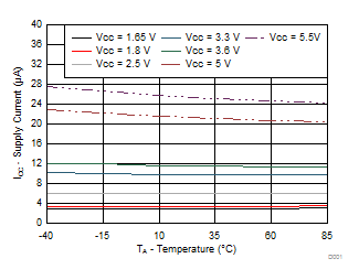
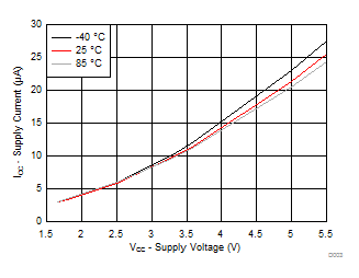
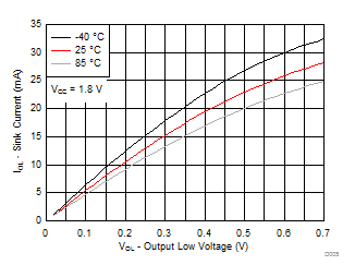
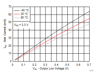
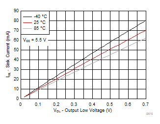
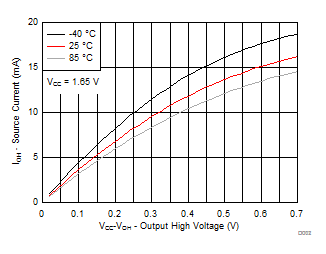
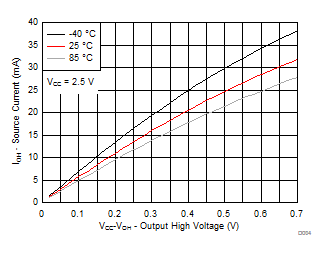
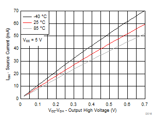
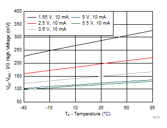
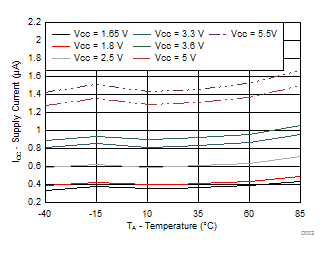
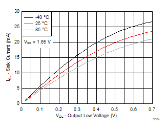
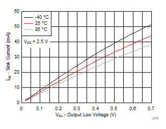
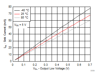
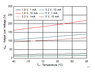
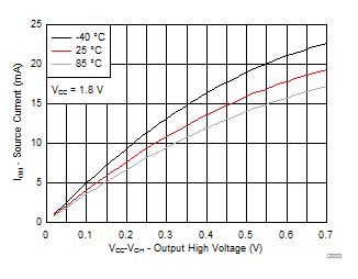
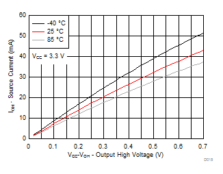
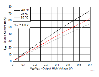
TA = 25°C (unless otherwise noted)