SBVA072A December 2020 – January 2021 TPS3703-Q1
4 Pin Failure Mode Analysis (Pin FMA)
This section provides a Failure Mode Analysis (FMA) for the pins of the TPS3703-Q1. The failure modes covered in this document include the typical pin-by-pin failure scenarios:
- Pin short-circuited to Ground (see Table 4-2)
- Pin open-circuited (see Table 4-3)
- Pin short-circuited to an adjacent pin (see Table 4-4)
- Pin short-circuited to VDD (see Table 4-5)
- Pin short-circuited to /RESET is also included (see Table 4-6)
Table 4-2 through Table 4-6 also indicate how these pin conditions can affect the device as per the failure effects classification in Table 4-1.
| Class | Failure Effects |
|---|---|
| A | Potential device damage that affects functionality |
| B | No device damage, but loss of functionality |
| C | No device damage, but performance degradation |
| D | No device damage, no impact to functionality or performance |
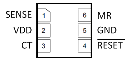
Figure 4-1 shows the TPS3703-Q1 pin diagram. For a detailed description of the device pins please refer to the Pin Configuration and Functions section in the TPS3703-Q1 data sheet.
 Figure 4-1 Pin DiagramDSE Package6-Pin WSON
Following are the assumptions of use and the device configuration assumed for the pin FMA in this section:
- VDD = 3.3 V, V_SENSE = 1.2 V, /RESET pulled-up to VDD unless stated otherwise
| Pin Name | Pin No. | Description of Potential Failure Effect(s) | Failure Effect Class |
|---|---|---|---|
| SENSE | 1 | No damage to device, can affect application functionality. Shorts voltage supply to ground, increases current. | C |
| VDD | 2 | No damage to device, can affect application functionality. Shorts voltage supply to ground, increases current. | C |
| CT | 3 | Normal operation, device in Latch mode. Usually has pull-down resistance to limit currEnt | D |
| /RESET | 4 | No damage to device, can affect application functionality. Forces /reset to be asserted. | C |
| GND | 5 | Normal operation. | D |
| /MR | 6 | Normal operation in some cases, but forces /reset to be asserted. | C |
| Pin Name | Pin No. | Description of Potential Failure Effect(s) | Failure Effect Class |
|---|---|---|---|
| SENSE | 1 | No damage to device, can affect application functionality. /Reset tends to be low. | C |
| VDD | 2 | No damage to device, but device is unpowered. /Reset tends to be low. | C |
| CT | 3 | Normal operation. | D |
| /RESET | 4 | Open drain output requires pull-up voltage for functionality. | C |
| GND | 5 | No damage to device, but device is unpowered. /Reset tends to be low. | C |
| /MR | 6 | Normal operation. Pin is internally pulled up to VDD. | D |
| Pin Name | Pin No. | Shorted to | Description of Potential Failure Effect(s) | Failure Effect Class |
|---|---|---|---|---|
| SENSE | 1 | VDD | Normal operation in some applications. Functionality affected with separate supply for sense, but no damage. | C |
| VDD | 2 | CT | Normal operation. Usually has pull-up resistance to limit current. | D |
| CT | 3 | /RESET | No damage to device, but device is unpowered. /Reset tends to be low. | C |
| /RESET | 4 | GND | No damage to device, can affect application functionality. Forces /reset to be asserted. | C |
| GND | 5 | /MR | Normal operation in some cases, but forces /reset to be asserted. | C |
| /MR | 6 | SENSE | Undefined operation, but functionality can be affected. When MR is asserted, SENSE will short to GND. | C |
| Pin Name | Pin No. | Description of Potential Failure Effect(s) | Failure Effect Class |
|---|---|---|---|
| SENSE | 1 | Normal operation in some applications. Functionality affected with separate supply for sense, but no damage. | C |
| VDD | 2 | Normal operation. | D |
| CT | 3 | Normal operation. Usually has pull-up resistance to limit current. | D |
| /RESET | 4 | Normal operation. Usually has pull-up resistance to limit current. | D |
| GND | 5 | No damage to device, can affect application functionality. Shorts voltage supply to ground, increases current. | C |
| /MR | 6 | Normal operation, but increased leakage current. Internally pulled-up to VDD to limit current. | D |
| Pin Name | Pin No. | Description of Potential Failure Effect(s) | Failure Effect Class |
|---|---|---|---|
| SENSE | 1 | No damage to device, can affect application functionality. Forces /reset to equal sense voltage. | C |
| VDD | 2 | Normal operation. Usually has pull-up resistance to limit current. | D |
| CT | 3 | No damage to device, can affect application functionality. /Reset tends to be low. | C |
| /RESET | 4 | Normal operation. | D |
| GND | 5 | No damage to device, can affect application functionality. Forces /reset to be asserted. | C |
| /MR | 6 | No damage to device, can affect application functionality. Forces /RESET to latch. | C |