SBOU252 August 2021
4.1 Schematic
Figure 4-1 displays the DYY-AMP-EVM circuit schematic.
Figure 4-1 DYY-AMP-EVM Schematic
Table 4-1 DYY-AMP-EVM Components
| CH | RINM | RF | CF | RINP | RVREF | CVREF | RPL | RIso | CL |
|---|---|---|---|---|---|---|---|---|---|
| 1 | R1 | R2 | C3 | R3 | R4 | C4 | R6 | R5 | C5 |
| 2 | R7 | R8 | C6 | R9 | R10 | C7 | R12 | R11 | C8 |
| 3 | R13 | R14 | C9 | R15 | R16 | C10 | R18 | R17 | C11 |
| 4 | R19 | R20 | C12 | R21 | R22 | C13 | R24 | R23 | C14 |
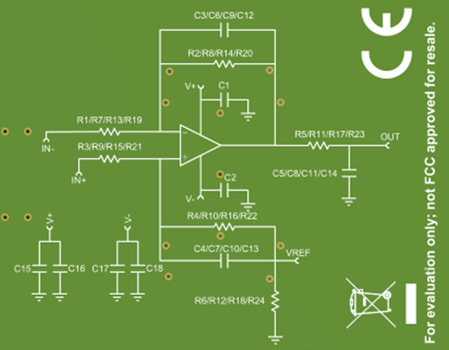
The schematic of the EVM is provided in silk screen located on the back of the PCB for easy reference. Figure 4-2 displays the schematic provided on the back of the PCB.
 Figure 4-2 Silkscreen Schematic