SBOA519 June 2021 INA240
2 Output Swing in Current Sense Amplifiers
A mistake that is often made with regard to swing limitations is that they are treated as a static condition, if considered at all. Commonly, swing test conditions can often be found in the Electrical Characteristics table of a current sense amplifier data sheet, such is in Figure 2-1.
 Figure 2-1 INA240 Output Swing
Limitations
Figure 2-1 INA240 Output Swing
LimitationsExamining this information from the INA240 High- and Low-Side, Bidirectional, Zero-Drift, Current-Sense Amplifier With Enhanced PWM Rejection Data Sheet, several observations are obtained. First, the output of the amplifier is not ideal to the supply, but rather is only capable of swinging to 4.8 V in the worst case (4.95 V typical) condition for a supply of 5 V. The same observation is also made regarding the device's ability to swing to GND. This information demonstrates that, should the device be operated in a unidirectional manner, that is, the REF pins of the INA240 both set to GND, that the output is not capable of truly measuring 0 A. (A true drive to 0 A is possible in a unidirectional setup, however, if the reference is used to pedestal above the swing condition. This comes at the loss of a small amount of dynamic range.)
These conditions do not hold true for the entirety of the potential load range, however. As required load current increases, this often comes at the expense of output swing head room of the device. The conditions above only examine swing on the output of the device in a single location for potential loading, in this case 10kΩ to GND. Should the loading of the output change, and more current is demanded, this can potentially alter the output stage's swing characteristics, and lead to saturation against the rail if not properly designed for. A good example to imagine here is a step in load current at the output of the current sense amplifier. The designer needs to ensure that the largest load current is taken into account with respect to desired full scale range to ensure that the output of the device is capable of handling this change.
Load resistance and the maximum desired output voltage for the output stage allow the engineer to calculate the maximum current required by the load. For example, in the data sheet test condition discussed above, the maximum output capable is 4.8 V, and the load resistance is 10 kΩ. If a design were in motion with these desired parameters, then maximum current sourced by the output can be calculated as:
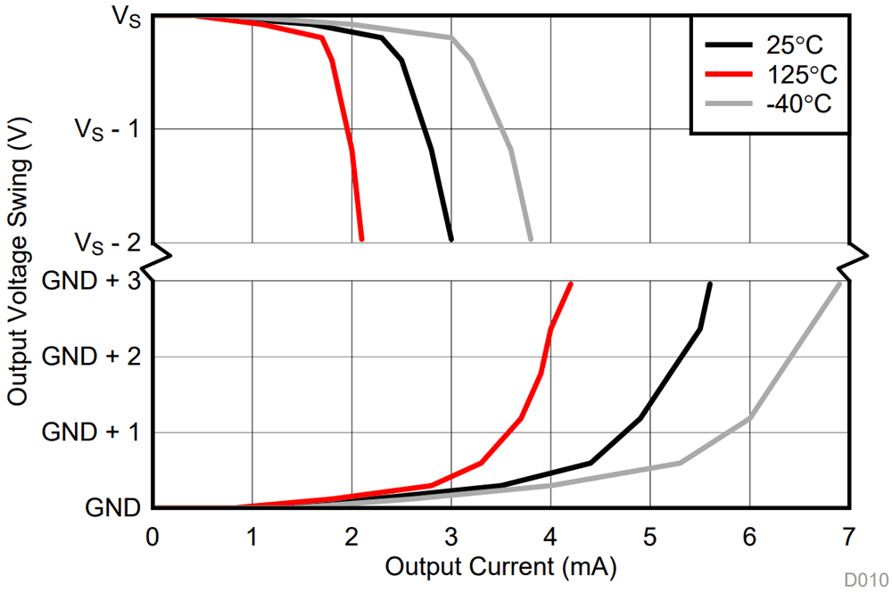
For the Texas Instruments' amplifier portfolio, this information across the load current range is typically conveyed in a common figure referred to as the "claw" curve, as they somewhat resemble animal claws. Figure 2-2 shows the claw curve of the INA240.
 Figure 2-2 INA240 Output Voltage Swing vs
Output Current Capability
Figure 2-2 INA240 Output Voltage Swing vs
Output Current CapabilityThese curves are normally divided into a top and bottom section, and the above curve is no different. The upper family of curves demonstrates the devices ability to source current, while the lower family of curves gives the device's ability to sink current. Information is also provided at the ambient temperature point, and the extremes of the device's temperature range. Some devices may include additional temperature curves, but these three datasets will normally be provided at a minimum.
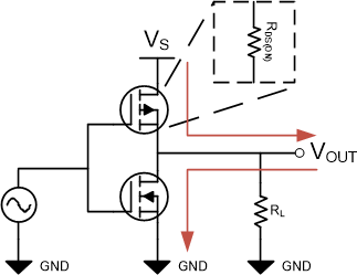
Breaking down the curves, you can again make several observations. First, it can be seen that as the desired load current grows, the ability of the device to swing completely to the rail diminishes. This is due to the fact that, for CMOS output stages, as load current increases through the FET, and a drop is created over the RDS(ON) of the FET that will scale with the output current of the device. This is visualized in a high level diagram in Figure 2-3.
 Figure 2-3 CMOS Output Stage and Load Current
Flow
Figure 2-3 CMOS Output Stage and Load Current
FlowNext, this relationship is not linear across the entire range, and a portion of the curve is reached where significant falloff is observed. This is due to the fact that the RDS(ON) of the FETs is not a linear process, and increases with increasing current from drain to source.
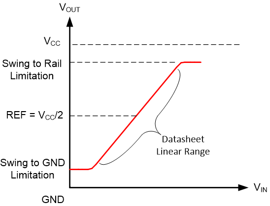
Finally, an important aspect of these curves to understand is that these curves are not meant to be interpreted as a simple "translational" relationship as the claw curve limit is reached. Typically, a good design rule is to provide some amount of headroom away from the hard limit of the claw curve. While amplifier output stages are relatively linear to a point, there are diminishing returns as the rail is approached, and components of both the linear area and saturation area will be present in the output. Figure 2-4 shows a typical FET curve is demonstrated to help visualize this in .
 Figure 2-4 Typical Current Sense Amplifier
Output Curve
Figure 2-4 Typical Current Sense Amplifier
Output CurveFor this reason, it is typically recommended that a small amount of margin be built into the design to work away from the hard value shown in the claw curve, nominally a few tens to hundreds of millivolts.