SNAS449F February 2008 – May 2017 DAC081C081 , DAC081C085
PRODUCTION DATA.
- 1 Features
- 2 Applications
- 3 Description
- 4 Revision History
- 5 Description (continued)
- 6 Pin Configuration and Functions
- 7 Specifications
- 8 Detailed Description
- 9 Application and Implementation
- 10Power Supply Recommendations
- 11Layout
- 12Device and Documentation Support
- 13Mechanical, Packaging, and Orderable Information
1 Features
- Ensured Monotonicity to 8-bits
- Low Power Operation: 156 µA Maximum at 3.3 V
- Extended Power Supply Range (2.7 V to 5.5 V)
- I2C-Compatible 2-Wire Interface Which Supports Standard (100-kHz), Fast (400-kHz), and High-Speed (3.4-MHz) Modes
- Rail-to-Rail Voltage Output
- Very Small Package
- Resolution 8 Bits
- INL ±0.6 LSB (Maximum)
- DNL ±0.1 LSB (Maximum)
- Settling Time 4.5 μs (Maximum)
- Zero Code Error +10 mV (Maximum)
- Full-Scale Error −0.7 %FS (Maximum)
- Supply Power
- Normal
- 380 μW (3 V)
- 730 μW (5 V) Typical
- Power Down
- 0.5 μW (3 V)
- 0.9 μW (5 V) Typical
- Normal
2 Applications
- Industrial Process Control
- Portable Instruments
- Digital Gain and Offset Adjustments
- Programmable Voltage and Current Sources
- Test Equipment
3 Description
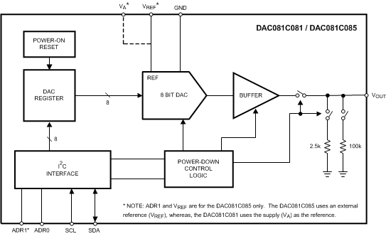
The DAC081C08x device is an 8-bit, single-channel, voltage-output digital-to-analog converter (DAC) that operates from a 2.7-V to 5.5-V supply. The output amplifier allows rail-to-rail output swing and has an 4.5-µsec settling time. The DAC081C081 uses the supply voltage as the reference to provide the widest dynamic output range and typically consumes 132 µA while operating at 5 V. It is available in 6-lead SOT and WSON packages and provides three address options (pin selectable).
As an alternative, the DAC081C085 provides nine I2C addressing options and uses an external reference. It has the same performance and settling time as the DAC081C081. It is available in an 8-lead VSSOP.
The DAC081C081 and DAC081C085 use a 2-wire, I2C-compatible serial interface that operates in all three speed modes, including high-speed mode (3.4 MHz). An external address selection pin allows up to three DAC081C081 or nine DAC081C085 devices per 2-wire bus. Pin-compatible alternatives to the DAC081C081 are available that provide additional address options.
Table 1. Device Information(1)
| PART NUMBER | PACKAGE | BODY SIZE (NOM) |
|---|---|---|
| DAC081C081 | WSON (6) | 2.20 mm × 2.50 mm |
| SOT (6) | 1.60 mm × 2.90 mm | |
| DAC081C085 | VSSOP (8) | 3.00 mm × 3.00 mm |
- For all available packages, see the orderable addendum at the end of the data sheet.
3.1 Block Diagram
