SLUSC99A July   2016  – January 2017 UCD3138128A

PRODUCTION DATA.  

  1. Features
  2. Applications
  3. Description
  4. Revision History
  5. Device Comparison
  6. Pin Configuration and Functions
  7. Specifications
    1. 7.1 Absolute Maximum Ratings
    2. 7.2 ESD Ratings
    3. 7.3 Recommended Operating Conditions
    4. 7.4 Thermal Information
    5. 7.5 Electrical Characteristics
    6. 7.6 Timing Characteristics
    7. 7.7 PMBus/SMBus/I2C Timing
    8. 7.8 Typical Characteristics
    9. 7.9 Timing Diagrams
  8. Parametric Measurement Information
    1. 8.1 Typical Clock Gating Power Savings
  9. Detailed Description
    1. 9.1 Overview
      1. 9.1.1 ARM Processor
      2. 9.1.2 Memory
    2. 9.2 Functional Block Diagram
    3. 9.3 Feature Description
      1. 9.3.1  System Module
        1. 9.3.1.1 Address Decoder (DEC)
        2. 9.3.1.2 Memory Management Controller (MMC)
        3. 9.3.1.3 System Management (SYS)
        4. 9.3.1.4 Central Interrupt Module (CIM)
      2. 9.3.2  Peripherals
        1. 9.3.2.1 Digital Power Peripherals (DPPs)
          1. 9.3.2.1.1 Front End
          2. 9.3.2.1.2 DPWM Module
          3. 9.3.2.1.3 DPWM Events
          4. 9.3.2.1.4 High Resolution DPWM
          5. 9.3.2.1.5 Oversampling
          6. 9.3.2.1.6 DPWM Interrupt Generation
          7. 9.3.2.1.7 DPWM Interrupt Scaling/Range
          8. 9.3.2.1.8 Synchronous Rectifier Dead Time Optimization Peripheral
      3. 9.3.3  Automatic Mode Switching
        1. 9.3.3.1 Phase Shifted Full Bridge Example
        2. 9.3.3.2 LLC Example
        3. 9.3.3.3 Mechanism For Automatic Mode Switching
      4. 9.3.4  DPWMC, Edge Generation, Intramux
      5. 9.3.5  Synchronous Rectifier MOSFET Ramp And IDE Calculation
      6. 9.3.6  Filter
        1. 9.3.6.1 Loop Multiplexer
        2. 9.3.6.2 Fault Multiplexer
      7. 9.3.7  Communication Ports
        1. 9.3.7.1 SCI (UART) Serial Communication Interface
        2. 9.3.7.2 PMBUS/I2C
          1. 9.3.7.2.1 Example: PMBus Address Decode via ADC12 Reading
        3. 9.3.7.3 SPI
        4. 9.3.7.4 JTAG Standard Interface
      8. 9.3.8  Real Time Clock
      9. 9.3.9  External Crystal Interface
      10. 9.3.10 Timers
        1. 9.3.10.1 24-Bit Timer
        2. 9.3.10.2 16-Bit PWM Timers
        3. 9.3.10.3 Watchdog Timer
      11. 9.3.11 General Purpose ADC12
      12. 9.3.12 Miscellaneous Analog
      13. 9.3.13 Brownout
      14. 9.3.14 Global I/O
      15. 9.3.15 Temperature Sensor Control
      16. 9.3.16 I/O Mux Control
      17. 9.3.17 Current Sharing Control
      18. 9.3.18 Temperature Reference
    4. 9.4 Device Functional Modes
      1. 9.4.1 DPWM Modes of Operation
        1. 9.4.1.1 Normal Mode
        2. 9.4.1.2 DPWM Multiple Output Mode
        3. 9.4.1.3 DPWM Resonant Mode
        4. 9.4.1.4 Triangular Mode
        5. 9.4.1.5 Leading Edge Mode
        6. 9.4.1.6 Phase Shifting
    5. 9.5 Register Maps
      1. 9.5.1 CPU Memory Map And Interrupts
        1. 9.5.1.1 Memory Map (After Reset Operation)
        2. 9.5.1.2 Memory Map (Normal Operation)
        3. 9.5.1.3 Memory Map (System And Peripherals Blocks)
      2. 9.5.2 Boot ROM
        1. 9.5.2.1 Pseudo Code for ROM
      3. 9.5.3 Customer Boot Program
      4. 9.5.4 Flash Management
  10. 10Applications and Implementation
    1. 10.1 Application Information
    2. 10.2 Typical Application
      1. 10.2.1 Design Requirements
      2. 10.2.2 Detailed Design Procedure
        1. 10.2.2.1 PCMC (Peak Current Mode Control) PSFB (Phase Shifted Full Bridge) Hardware Configuration Overview
        2. 10.2.2.2 DPWM Initialization for PSFB
        3. 10.2.2.3 DPWM Synchronization
        4. 10.2.2.4 Fixed Signals to Bridge
        5. 10.2.2.5 Dynamic Signals to Bridge
      3. 10.2.3 System Initialization for PCM
        1. 10.2.3.1 Use of Front Ends and Filters in PSFB
        2. 10.2.3.2 Peak Current Detection
        3. 10.2.3.3 Peak Current Mode (PCM)
      4. 10.2.4 Application Curves
  11. 11Power Supply Recommendations
  12. 12Layout
    1. 12.1 Device Grounding and Layout Guidelines
    2. 12.2 Layout Examples
  13. 13Device and Documentation Support
    1. 13.1 Device Support
      1. 13.1.1 Development Support
    2. 13.2 Documentation Support
      1. 13.2.1 Related Documentation
        1. 13.2.1.1 References
    3. 13.3 Receiving Notification of Documentation Updates
    4. 13.4 Trademarks
    5. 13.5 Electrostatic Discharge Caution
    6. 13.6 Glossary
  14. 14Mechanical, Packaging, and Orderable Information

封装选项

机械数据 (封装 | 引脚)
散热焊盘机械数据 (封装 | 引脚)
订购信息

Layout

Device Grounding and Layout Guidelines

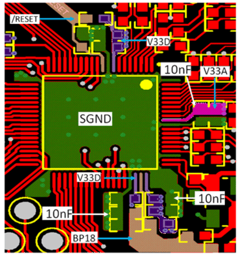
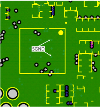
  • Single ground is recommended: SGND. A multilayer such as 4 layers board is recommended so that one solid SGND is dedicated for return current path, referred to the layout example.
  • Apply multiple different capacitors for different frequency range on decoupling circuits. Each capacitor has different ESL, Capacitance and ESR, and they have different frequency response.
  • Avoid long traces close to radiation components, and place them into an internal layer, and it is preferred to have grounding shield.
  • Analog circuits and digital circuits should have separate return to ground; although with a single plane, still try to avoid mixing analog current and digital current.
  • Do not use a ferrite bead or larger than 3-Ω resistor to connect between V33A and V33D.
  • Both 3.3VD and 3.3VA should have local decoupling capacitors close to the device power pins, add vias to connect decoupling caps directly to SGND.
  • Avoid negative current/negative voltage on all pins, so Schottky clamping diodes may be needed to limit the voltage; avoid more than 3.8 V or less than –0.3 V voltage spikes on all pins; add Schottky diodes on the pins which could have voltage spikes during surge test; be aware that a Schottky has relatively higher leakage current, which can affect the voltage sensing at high temperature.
  • If V33 slew rate is less than 2.5 V/ms the RESET pin should have a 2.21-kΩ resistor between the reset pin and V33D and a 2.2-µF capacitor from RESET to ground. For more details please refer to the UCD3138 Family - Practical Design Guideline This capacitor must be located close to the device RESET pin.
  • If the XTAL_IN (Pin 61) and XTAL_OUT (Pin 62) are not used for external clock, tie them to 1.8 V (Pin BP18) through a 1-kΩ resistor respectively.
  • Configure unused GPIO pins to be inputs or connect them to the ground (DGND or SGND); when an external pull-up resistor is used for GPIO, the pull-up resistor needs to be 1 kΩ or higher.

For detailed practical design guidelines, refer to (UCD3138 Family - Practical Design Guideline).
Layout Examples

UCD3138128A PCB_layer1_slusc99.gif Figure 53. Layout Example for UCD3138128A Top Layer
UCD3138128A PCB_layer2_slusc99.gif Figure 54. Layout Example for UCD3138128A Internal Ground Layer