ZHCSPH5C June 2022 – March 2023 UCC28C50 , UCC28C51 , UCC28C52 , UCC28C53 , UCC28C54 , UCC28C55 , UCC28C56H , UCC28C56L , UCC28C57H , UCC28C57L , UCC28C58 , UCC28C59 , UCC38C50 , UCC38C51 , UCC38C52 , UCC38C53 , UCC38C54 , UCC38C55
PRODUCTION DATA
9.2.2.10.4 补偿环路
补偿回路的设计涉及到选择适当的元件,以便可以设计所需的增益、极点和零点,从而得到在整个工作范围内稳定工作的系统。环路有三个不同的部分:TL431、光耦合器和误差放大器。这些电路级每个都与功率级相结合,以形成稳定且稳健的系统。
为了获得良好的瞬态响应,最终设计的带宽必须尽可能大。使用方程式 41,CCM 反激式的带宽 fBW 被限制为 RHP 零点频率的 ¼,或大概为 1.77kHz。

可以使用方程式 40 计算或在波特图(图 9-4)上观察到开环功率级在 fBW 处的增益,该增益等于 -19.55dB,且 fBW 处的相位等于 -58°。
补偿回路的次级侧部分首先建立调节后的稳态输出电压。为了设置稳压输出电压,TL431 可调节精密并联稳压器由于其精确的电压基准和内部运算放大器,因此非常适合在隔离变流器的次级侧使用。根据所需功耗选择从转换器输出端子到 TL431 REF 引脚的分压器中使用的电阻器。由于 TL431 的 REF 输入电流仅为 2µA,因此为 1mA 的分压器电流 (IFB_REF) 选择电阻器所产生的误差将极小。顶部分压器电阻 RFBU 使用以下公式计算:

TL431 基准电压 (REFTL431) 的典型值为 2.495V。为 RFBU 选用 9.53kΩ 电阻器。为了将输出电压设置为 12V,为 RFBB 使用 2.49kΩ。

为了获得良好的相位裕度,需要一个补偿器零点 (fCOMPz),并且应将其放置在所需带宽的 1/10 处:


使用该转换器,fCOMPz 应设置为大概 177Hz。放置在 TL431 阴极至 REF 之间的串联电阻器 (RCOMPz) 和电容器 (CCOMPz) 设置补偿器零点位置。将 CCOMPz 设置为 0.01µF,RCOMPz 可以使用以下公式计算:

对 RZ 使用 88.7kΩ 的标准值并对 CZ 使用 0.01µF,可得出零点位于 179Hz 处。
在图 9-3 中,RTLbias 通过齐纳二极管 (DREG) 提供的调节电压为 TL431 提供阴极电流。为了实现稳健的性能,通过 10V 齐纳提供 10mA 来偏置 TL431,并对 RTLbias 使用 1kΩ 电阻器。
补偿回路的 TL431 部分的增益可使用方程式 47 来计算。

在右半平面零点或 ESR 零点的频率(以最低者为准)处需要一个补偿极点。根据之前的分析,右半平面零点 (fRHPz) 位于 7.07kHz 处,ESR 零点 (fESRz) 位于 1.68kHz 处;因此,对于这种设计,补偿极点必须设置在 1.68kHz 处。光耦合器包含一个难以在频率上表征的寄生极,因此该光耦合器设置了一个下拉电阻器,即 ROPTO 等于 1kΩ,这使得寄生光耦合器极进一步移出,超出了本设计的关注范围。
可以使用 RCOMPp 和 CCOMPp 将所需的补偿极点添加到初级侧误差放大器中。选择 RCOMPp 为 10kΩ,使用方程式 48 确定 CCOMPp 的所需值。

CCOMPp 使用 10nF 电容器来将补偿极点设置为 1.59kHz。
可能需要在初级侧误差放大器上添加直流增益,以获得所需的带宽,并有助于根据需要调整环路增益。RFBG 使用 4.99kΩ 来将误差放大器上的直流增益设置为 2。此时,补偿回路的误差放大器级的增益传递函数 (GEA(s)) 可以使用方程式 49 来表征:

使用电流传输比 (CTR) 通常在相关频率范围内为 100% 的光耦合器,以便 CTR=1,光耦合器级的传递函数 (GOPTO(s)) 为方程式 50。

至光耦合器内部二极管的偏置电阻器 (RLED) 和光发射器上的下拉电阻器 (ROPTO) 设置跨隔离边界的增益。ROPTO 已设置为 1kΩ,但 RLED 的值尚未确定。
总闭环增益 (GTOTAL(s)) 是开环功率级 (Ho(s))、光增益 (GOPTO(s))、误差放大器增益 (GEA(s)) 和 TL431 级增益 (GTL431(s)) 的组合,如方程式 51 中所示。

可以选择 RLED 的所需值以实现所需的交叉频率 (fBW)。通过在所需的交叉频率处将总环路增益设置为 1 并重新排列方程式 51,可以确定 RLED 的最优值,如方程式 52 所示。

1.3kΩ 电阻器适合 RLED 的要求。
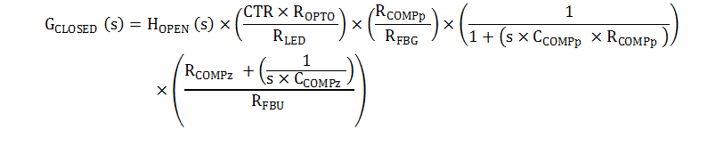
基于补偿环路结构,将整个补偿环路传递函数写成方程式 53。
最终的闭环波特图如图 9-6 和图 9-7 所示。该转换器实现的交叉频率大概为 1.8kHz,相位裕度大概为 67°。
TI 建议检查所有临界情况下的环路稳定性,包括元件公差,以确保系统稳定性。
 图 9-6 转换器闭环波特图 - 增益
 图 9-7 转换器闭环波特图 - 相位