ZHCSCD4B July 2013 – August 2014 UCC28910
PRODUCTION DATA.
- 1 特性
- 2 应用范围
- 3 说明
- 4 简化电路原理图 简化电路原理图
- 5 修订历史记录
- 6 Terminal Configuration and Functions
- 7 Specifications
-
8 Detailed Description
- 8.1 Overview
- 8.2 Functional Block Diagram
- 8.3 Detailed Device Description
- 8.4 Feature Description
- 8.5 Device Functional Modes
-
9 Applications and Implementation
- 9.1 Application Information
- 9.2
Typical Application
- 9.2.1
Battery Charger, 5 V, 6 W
- 9.2.1.1 Design Requirements
- 9.2.1.2
Detailed Design Procedure
- 9.2.1.2.1 Power Handling Curves
- 9.2.1.2.2 Definition of Terms
- 9.2.1.2.3 Maximum Target Switching Frequency
- 9.2.1.2.4 Transformer Turns Ratio, Inductance, Primary-Peak Current
- 9.2.1.2.5 Bulk Capacitance
- 9.2.1.2.6 Output Capacitance
- 9.2.1.2.7 VDD Capacitance, CVDD
- 9.2.1.2.8 VS Resistor Divider
- 9.2.1.2.9 RVDD Resistor and Turn Ratio
- 9.2.1.2.10 Transformer Input Power
- 9.2.1.2.11 RIPK Value
- 9.2.1.2.12 Primary Inductance Value
- 9.2.1.2.13 Pre-Load
- 9.2.1.2.14 DRAIN Voltage Clamp Circuit
- 9.2.1.3 Application Curves
- 9.2.1.4 Average Efficiency Performance and Standby Power of the UCC28910FBEVM-526
- 9.2.1
Battery Charger, 5 V, 6 W
- 10Power Supply Recommendations
- 11Layout
- 12器件和文档支持
- 13机械封装和可订购信息
9 Applications and Implementation
9.1 Application Information
The UCC28910 device is a HV switcher that integrates an HV power FET plus a controller that uses primary-side-regulated (PSR), supporting magnetically-sensed output voltage regulation via the transformer bias winding. This sensing eliminates the need for a secondary-side reference, error amplifier and optical-isolator for output voltage regulation. The device delivers accurate output voltage static load and line regulation, and accurate control of the output current. The magnetic sampling scheme allows operation only in discontinuous conduction mode (DCM) so the device is not allowed to turn on the Power FET if it doesn’t sense a ZCD event that is when auxiliary winding voltage crosses zero from high to low after transformer demagnetization is complete. The modulator adjusts both frequency and peak current in different load regions to maximize efficiency throughout the operating range. The smart management of the control logic power consumption and the HV current source, used for startup that is off during operation and have very low leakage current, allow designing converters with very low standby input power. The less than 30mW can be easily achieved with this device.
9.2 Typical Application
9.2.1 Battery Charger, 5 V, 6 W
This design example describes the UCC28910FBEVM-526 design and outlines the design steps required to design a constant-voltage, constant-current flyback converter for a 5-V/6-W charger. Discontinuous conduction mode (DCM) with valley switching is used to reduce switching losses. A combination of switching frequency and peak primary current amplitude modulation is used to keep conversion efficiency high across the full load and input voltage range. Figure 25 below details the output V-I characteristic. Low system parts count and built in advanced protection features result in a cost-effective solution that meets stringent world-wide energy efficiency requirements.
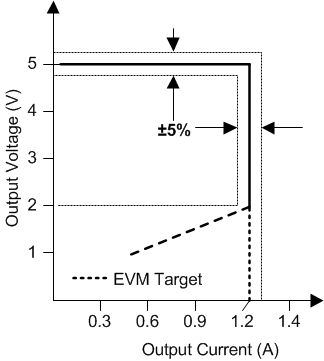 Figure 25. Target Output V-I Characteristic
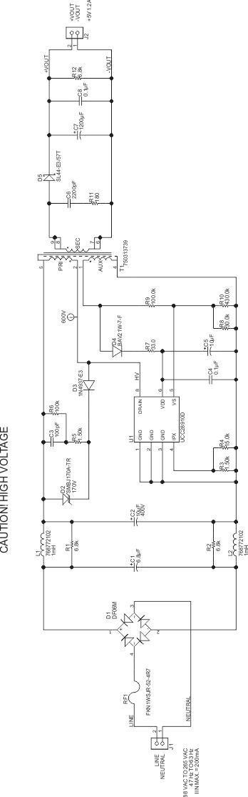 Figure 26. UCC28910FBEVM-526 Schematic
9.2.1.1 Design Requirements
For this design example, use the parameters listed in Table 1.
Table 1. Design Parameters
| PARAMETER | TEST CONDITIONS | MIN | TYP | MAX | UNIT | |
|---|---|---|---|---|---|---|
| INPUT CHARACTERISTICS | ||||||
| VIN | Input voltage | 85 | 115/230 | 265 | V | |
| fLINE | Frequency | 47 | 50/60 | 64 | Hz | |
| PNL | No load power | VIN = VNOM IOUT = 0 A | 15 | 20 | mW | |
| VINUVLO | Brownout voltage | IOUT = INOM | 70 | V | ||
| VINOV | Brownout recovery voltage | 80 | V | |||
| IIN | Input current | VIN = VMIN, IOUT = max | 0.2 | A | ||
| OUTPUT CHARACTERISTICS | ||||||
| VOUT | Output voltage | VIN =VMIN to VMAX, IOUT = 0 V to INOM | 4.75 | 5.00 | 5.25 | V |
| IOUT(max) | Maximum output current | VIN = VMIN to VMAX | 1.14 | 1.20 | 1.26 | A |
| IOUT(min) | Minimum output current | Vin = Vmin to VMAX | 0 | A | ||
| ΔVOUT | Output voltage ripple | VIN = VMIN to VMAX, IOUT = 0 V to INOM | 150 | mV | ||
| POUT | Output power | VIN = VMIN to VMAX | ||||
| SYSTEM CHARACTERISTICS | ||||||
| η | Average efficiency | 25%, 50%, 75%, 100% of IOUT | 75% | |||
| ENVIRONMENTAL | ||||||
| Conducted EMI | Meets CISPR22B/EN55022B | |||||
9.2.1.2 Detailed Design Procedure
This procedure outlines the steps to design a constant-voltage, constant-current flyback converter based on UCC28910 switcher. Refer to the Figure 27 for component names and network locations. The design procedure equations use terms that are defined below.
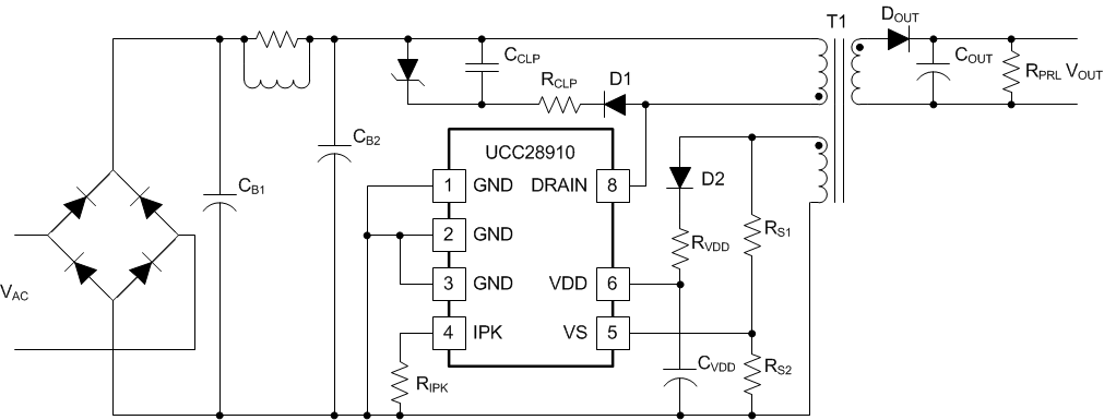 Figure 27. Standard Flyback Converter Based on UCC28910
9.2.1.2.1 Power Handling Curves
The application curves give the maximum input power that can be handled by the device versus the ambient temperature. Two input curves are shown below. The first refers to a wide-range input voltage (88 VAC; 264 VAC) converter; the second refers to a European range input voltage (175 VAC; 265 VAC) converter. The two curves refer to an AC / DC converter realized with the UCC28910 device using the provided design equations. A copper area, used as heat sink, connected to GND terminals, considered in calculation to get the Input curves is 560 mm2. The input stage losses are included. A full-bridge rectifier and 7.5 Ω as inrush limiter resistance was considered.
To estimate the maximum output power at a certain ambient temperature it is possible to multiply the input power given by the input curve by the estimated efficiency. Below are reported the output power curves where, as estimated efficiency, was considered the minimum required efficiency given by EPA in to the Eligible Criteria (Version 2.0) for single voltage external AC/DC power supplies to get energy star label.
The curves give a rough estimation of the power handling capability of the device because at the end this capability depends a lot from the other components used in the circuit. A big impact on efficiency and then, on power handling capability, is given by transformer. The primary-leakage inductance and primary-winding parasitic capacitance should be minimized to improve performance.
The output diode has also an important impact; better performance is generally obtained if a Schottky diode is used because of the low-forward voltage drop and fast switching times. The reverse leakage current of this diode has to be checked because this current, in the schottky diodes, is higher respect standard or fast diodes. It increases with temperature. If the revers current is too high it could cause thermal runaway of the diode beside of the additional losses. Considering the wide-range application (Figure 30) the point representing the required output power (6 W) and operating maximum TA (50°C) is below the 5-V curve so the device can handle the required power at the required condition.
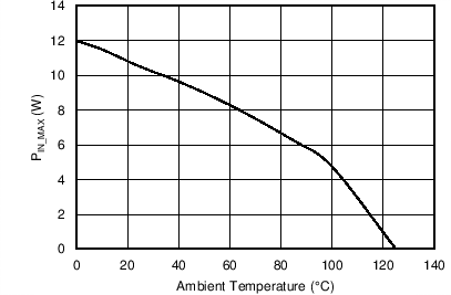 Figure 28. (90; 265) VRMS Input Voltage Range Converter Maximum Input Power vs Ambient Temperature
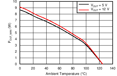 Figure 30. (90; 265) VRMS Input Voltage Range Converter Maximum Output Power vs Ambient Temperature
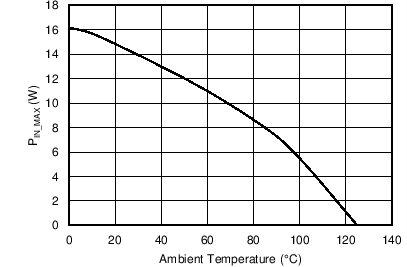 Figure 29. (180; 265) VRMS Input Voltage Range Converter Maximum Input Power vs Ambient Temperature
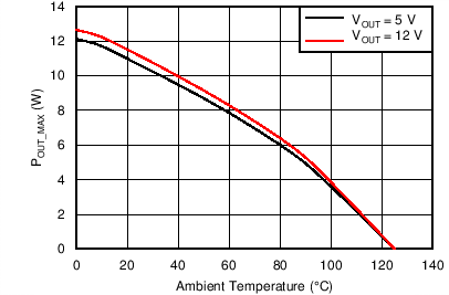 Figure 31. (180; 265) VRMS Input Voltage Range Converter Maximum Output Power vs Ambient Temperature
9.2.1.2.2 Definition of Terms
Capacitance Terms in Farads
- CBULK: total input capacitance of CB1 and CB2.
- CVDD: capacitance on the VDD terminal.
- COUT: output capacitance.
Duty Cycle Terms
- KCC: secondary diode conduction duty cycle in CC, (see Electrical Characteristics).
- DMAX: MOSFET on-time maximum duty cycle.
Frequency Terms in Hertz
- fLINE: minimum line frequency.
- fTARGET(max): target full-load maximum switching frequency of the converter.
- fMIN: minimum switching frequency of the converter, add 15% margin over the fSW(min) limit of the device.
- fSW(min): minimum switching frequency (see Electrical Characteristics)
Current Terms in Amperes
- IOCC: converter output current target when operating in constant current mode.
- ID_PK(max): maximum transformer primary current peak.
- ITRAN: required positive load-step current.
- IRUN: maximum current consumption of the device (see Electrical Characteristics).
- IVSLRUN: VS terminal run current (see Electrical Characteristics).
Current and Voltage Scaling Terms
- KAM: maximum-to-minimum peak-primary current ratio (see Electrical Characteristics).
Transformer Terms
- LP: transformer primary inductance.
- NPA: transformer primary-to-auxiliary turns ratio.
- NPS: transformer primary-to-secondary turns ratio.
Power Terms in Watts
- PIN: converter maximum input power.
- PINTRX: transformer maximum input power.
- POUT: full-load output power of the converter.
- PSB: total stand-by input power.
Resistance Terms in Ω
- RIPK: primary current programming resistance.
- RESR: total ESR of the output capacitors.
- RPRL: preload resistance on the output of the converter.
- RS1: high-side VS terminal resistance.
- RS2: low-side VS terminal resistance.
Timing Terms in Seconds
- tDMAG(min): minimum secondary rectifier conduction time.
- tON(min): minimum MOSFET on time.
- tR: resonant frequency during the DCM (discontinuous conduction mode) time.
Voltage Terms in Volts
- VBULK: highest bulk capacitor voltage for stand-by power measurement.
- VBULK(min): minimum voltage on CB1 and CB2 at full power.
- VCCR: constant-current regulating voltage (see Electrical Characteristics).
- VOΔ: output voltage drop allowed during the load-step transient.
- VDSPK: peak MOSFET drain-to-source voltage at high line.
- VF: secondary rectifier, DOUT, forward voltage drop at near-zero current.
- VFA: auxiliary rectifier, D2, forward voltage drop.
- VOCV: regulated output voltage of the converter, VOUT in CV mode.
- VVDD: voltage value on VDD terminal.
- VOCC: target lowest converter output voltage in constant-current regulation.
- VREV: peak reverse voltage on the secondary rectifier, DOUT.
- VRIPPLE: output peak-to-peak ripple voltage at full-load.
- VVSR: CV regulating level at the VS input (see Electrical Characteristics).
- ΔVUVLO: VDDON – VDDOFF (see Electrical Characteristics).
AC Voltage Terms in VRMS
- VIN(max): maximum AC input voltage to the converter.
- VIN(min): minimum AC input voltage to the converter.
- VIN(run): converter input start-up (run) AC voltage.
Efficiency Terms
- η: converter overall efficiency.
- ηXFMR: transformer primary-to-secondary power transfer efficiency.
9.2.1.2.3 Maximum Target Switching Frequency
The maximum operative switching frequency of the converter should be selected with a trade-off between the efficiency requirement (generally decreasing the switching frequency improves efficiency because the switching losses are reduced) and transformer size (increasing the switching frequency results in decreased transformer size). Some limits to the maximum value of the switching frequency need to be taken into account.
The internal oscillator of the device cannot exceed 115 kHz (see fSW(max) in the Electrical Characteristics) moreover the demagnetization time cannot be too short (tDMAG(min) > 1 μs) in order to allow for the proper working of the discriminator (see Primary-Side Voltage Regulation) and the maximum operative switching frequency is linked to the demagnetization time from the equation below.
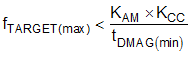
So the target maximum operative switching frequency of the converter satisfies to the below condition:
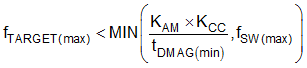
A good value for tDMAG(min) is 1.2 μs with some margin respect the minimum allowed value.
9.2.1.2.4 Transformer Turns Ratio, Inductance, Primary-Peak Current
The maximum primary-to-secondary turns ratio can be determined by the target maximum switching frequency at full load, the minimum input capacitor bulk voltage, and the estimated DCM quasi-resonant time. Initially determine the maximum available total duty cycle of the on-time and secondary conduction time based on target switching frequency and DCM resonant time. For DCM resonant time, assume tR = 1 / 500 kHz if you do not have an estimate from previous designs. For the transition mode operation limit, the period required from the end of secondary current conduction to the first valley of the VDS voltage is half of the DCM resonant period, or 1 μs assuming 500-kHz resonant frequency. DMAX can be determined using the equation below.
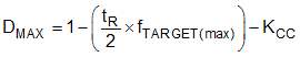
Once DMAX is known, the maximum turn ratio of the primary-to-secondary can be determined with the equation below.
DMAGCC is defined as the secondary diode conduction duty cycle during constant-current control mode operation. It is set internally by the UCC28910. This is the maximum allowable demagnetizing duty cycle and is equal to KCC. The total voltage on the secondary winding needs to be determined; the sum of VOCV and the secondary rectifier VF. The voltage VBULK(min) is generally selected around 65% or 60%. VBULK(min) is determined by the selection of the high-voltage input capacitors.
For the 5-V USB charger applications NPS values from 13 to 17 are typically used.
9.2.1.2.5 Bulk Capacitance
The minimum input capacitance voltage, the input power of the converter based on target full-load efficiency, minimum input RMS voltage, and minimum AC input frequency are used to determine the input capacitance requirement.
Maximum input power is determined based on VOCV, IOCC, and the full-load efficiency target.
The following equation provides an accurate solution for input capacitance based on a target minimum bulk capacitor voltage. To target a given input capacitance value, iterate the minimum capacitor voltage to achieve the target capacitance.
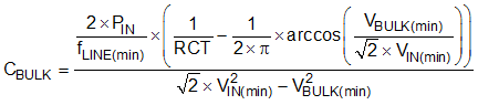
In the case the input rectifier is a single diode (half-wave rectifier) and for bridge-input rectifier (full-wave rectifier), as in the schematic of Figure 26.
9.2.1.2.6 Output Capacitance
The output capacitance value is typically determined by the transient response requirement from no load. For example, in USB charger applications, it is often required to maintain a minimum output voltage of 4.1 V with a load-step transient from 0 mA to 500 mA (ITRAN). The equation below assumes that the switching frequency can be at the UCC28910 minimum of fSW(min).
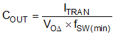
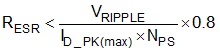
Another consideration on the output capacitor(s) is the ripple voltage requirement which is reviewed based on secondary-peak current and ESR. A margin of 20% is added to the capacitor ESR requirement in the equation below.
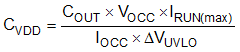
9.2.1.2.7 VDD Capacitance, CVDD
The capacitance on VDD needs to supply the device operating current until the output of the converter reaches the target minimum operating voltage in constant-current regulation. At this time the auxiliary winding can sustain the supply voltage to the UCC28910. The output current available to the load to charge the output capacitors is the constant-current regulation target. The equation below assumes the output current of the flyback is available to charge the output capacitance until the minimum output voltage is achieved.
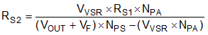
9.2.1.2.8 VS Resistor Divider
The VS divider resistors determine the output voltage regulation point of the flyback converter, also the high-side divider resistor (RS1) determines the line voltage at which the controller enables continuous switching operation. RS1 is initially determined based on transformer auxiliary to primary turn ratio and desired input voltage operating threshold.
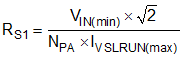
The low-side VS terminal resistor is selected based on desired output voltage regulation.
9.2.1.2.9 RVDD Resistor and Turn Ratio
The value of RVDD and the auxiliary-to-secondary turns ratio should be selected with care in order to be sure that the VDD is always higher than the VDDOFF (7 V maximum) threshold under all operating conditions. The RVDD resistor also limits the current that can go into the VDD terminal preventing IVDDCLP_OC clamp over-current protection from being erroneously activated.
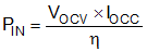
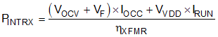
9.2.1.2.10 Transformer Input Power
The power at the transformer input during full-load condition is given by the output power plus the power loss in the output diode plus the power consumption of the UCC28910 control logic (VVDD × IRUN) divided by the transformer efficiency that takes into account all the losses due to the transformer: copper losses, core losses, and energy loss in the leakage inductances.
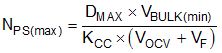
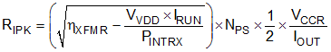
9.2.1.2.11 RIPK Value
The RIPK value sets the value of the DRAIN current peak that equals the transformer primary winding current peak value. This value also sets the value of the output current when working in CC mode according to the following formula:

where
- DMAGCC is the secondary diode conduction duty cycle
- NPS is the primary-to-secondary transformer turns ratio
- VCCR is the defined as VCCR = VCSTE(max) × KCC and the value is specified in the Electrical Characteristics
The term 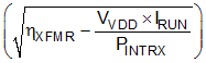 takes into account that not all the energy stored in the transformer goes to the secondary side but some of this energy, through the auxiliary winding, is used to supply the device control logic. The transfer of energy always happens with unavoidable losses. These losses are accounted for through the transformer efficiency term (ηXFMR). Fixed the target value for IOUT, the value of RIPK can be calculated using the following formula:
9.2.1.2.12 Primary Inductance Value
After you have fixed the maximum switching frequency and the maximum value of the primary current peak for your application, the primary inductance value can be fixed by the following equation:
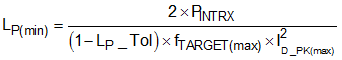
LP_Tol is the tolerance on the primary inductance value of the transformer. Typical values of LP_Tol are between ±10% and ±15%)
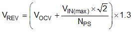
9.2.1.2.12.1 Secondary Diode Selection
The maximum reverse voltage that the secondary diode had to sustain can be calculated by the equation below where a margin of 30% is considered. Usually for this kind of application a Schottky diode is used to reduce the power losses due to the lower forward voltage drop. The maximum current rating of the diode is generally selected between two and five times the maximum output current (IOCC).
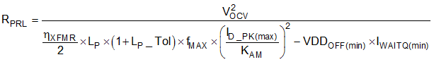
9.2.1.2.13 Pre-Load
When no load is applied on the converter output, the output voltage rises until the OVP (over voltage protection) of the device is tripped, because the device cannot operate at zero switching frequency. To avoid this, an RPRL (pre-load resistance) is used. The value of this pre-load can be selected using the following equation:
9.2.1.2.14 DRAIN Voltage Clamp Circuit
The main purpose of this circuit, as in most flyback converters, is to prevent the DRAIN voltage from rising up to the FET break-down voltage, at the FET turn-off, and destroying the FET itself. An additional task, required by the primary-side regulation mechanism, is to provide a clean input to UCC28910 VS terminal by damping the oscillation that is typically present on the DRAIN voltage due to the transformer primary leakage inductance.
To perform damping, the D1 diode selected is not a fast recovery diode (0.3 µs < tRR < 1 μs) so the reverse current can flow in the RLC over damped circuit. This RLC circuit is formed by the transformer primary leakage inductance (LLKP), the resistance RCLP, and the capacitance CCLP. To ensure proper damping the resistance RCLP has to satisfy the following condition:
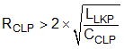
The capacitance CCLP should not be too high so it does not require too much energy to be charged. Typical values for CCLP are between 100 pF and 1 nF.
If the RCLP is too high, the additional drop on this resistance can cause excessively high DRAIN voltage. The DRAIN clamp circuit of Figure 27 can be modified as shown in Figure 32 where RCLP was divided into resistance (RCLP1 and RCLP2). Resistance RDCH can be added to discharge the CCLP capacitance before the next switching cycles. This can help in dumping oscillations caused by leakage inductance.
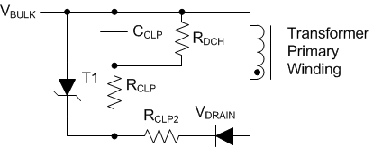 Figure 32. DRAIN Clamp Circuit Options
9.2.1.3 Application Curves
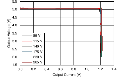 Figure 33. Output V-I Characteristic
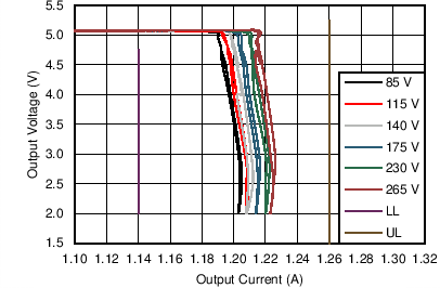 Figure 35. Output V-I Characteristic Output Voltage Regulation
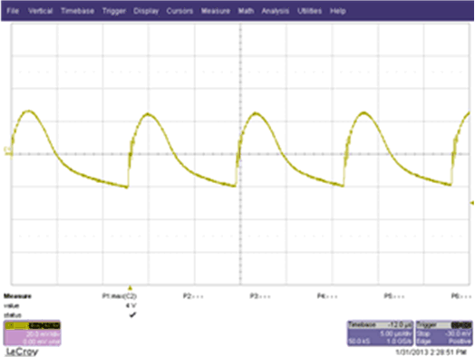 Figure 37. Ripple with 5-V, 1.2-A Output, 85 VAC Input,
 20 mV/div, 5 µs/div
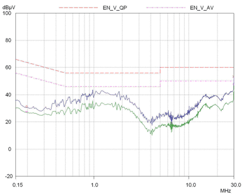 Figure 39. EMI Test Results per EN55022, Class B. 115 VAC Input
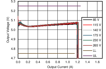 Figure 34. Output V-I Characteristic Output Current Regulation
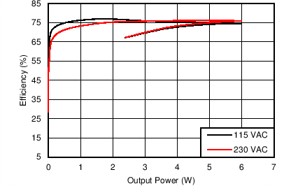 Figure 36. Efficiency vs POUT Diagram
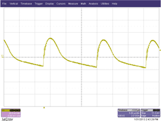 Figure 38. Ripple with 5-V,1.2-A Output, 265-VAC Input,
 20 mV/div 5 µs/div
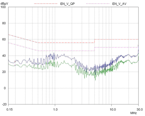 Figure 40. EMI Test Results per EN55022, Class B. 230-VAC Input
9.2.1.4 Average Efficiency Performance and Standby Power of the UCC28910FBEVM-526
Table 2 summarizes the average efficiency performance of the UCC28910FBEVM-526 and Table 3 summarizes the standby power that is the no-load power consumption of the converter.
Table 2. Average Efficiency Performance of the UCC28910FBEVM-526
| VIN (V) | f (Hz) | PIN (W) | IOUT (A) | VOUT (V) | POUT (W) | EFFICIENCY (%) | AVERAGE EFFICIENCY (%) |
|---|---|---|---|---|---|---|---|
| 115 | 60 | 7.826 | 1.201 | 4.950 | 5.943 | 75.94 | 76.25 |
| 5.845 | 0.901 | 4.942 | 4.451 | 76.15 | |||
| 3.889 | 0.601 | 4.934 | 2.964 | 76.19 | |||
| 1.930 | 0.301 | 4.927 | 1.481 | 76.73 | |||
| 230 | 50 | 7.721 | 1.201 | 4.956 | 5.950 | 77.06 | 76.68 |
| 5.783 | 0.901 | 4.948 | 4.457 | 77.07 | |||
| 3.853 | 0.601 | 4.938 | 2.966 | 76.97 | |||
| 1.960 | 0.301 | 4.930 | 1.482 | 75.60 |
Table 3. Standby Power, No-Load Power Consumption of the Converter
| VIN (V) | f (Hz) | PIN (mW) |
|---|---|---|
| 88 | 60 | 10 |
| 115 | 60 | 10 |
| 230 | 50 | 10 |
| 265 | 50 | 12 |