ZHCSAH7C November 2012 – June 2017 UCC28710 , UCC28711 , UCC28712 , UCC28713
PRODUCTION DATA.
- 1 特性
- 2 应用
- 3 说明
- 4 修订历史记录
- 5 Device Comparison Table
- 6 Pin Configuration and Functions
- 7 Specifications
- 8 Detailed Description
-
9 Application and Implementation
- 9.1 Application Information
- 9.2
Typical Application
- 9.2.1 Design Requirements
- 9.2.2
Detailed Design Procedure
- 9.2.2.1 Custom Design With WEBENCH® Tools
- 9.2.2.2 Stand-by Power Estimate
- 9.2.2.3 Input Bulk Capacitance and Minimum Bulk Voltage
- 9.2.2.4 Transformer Turns Ratio, Inductance, Primary-Peak Current
- 9.2.2.5 Transformer Parameter Verification
- 9.2.2.6 Output Capacitance
- 9.2.2.7 VDD Capacitance, CDD
- 9.2.2.8 VS Resistor Divider, Line Compensation, and Cable Compensation
- 9.2.3 Application Curves
- 10Power Supply Recommendations
- 11Layout
- 12器件和文档支持
- 13机械、封装和可订购信息
7 Specifications
7.1 Absolute Maximum Ratings
See (1).| MIN | MAX | UNIT | |||
|---|---|---|---|---|---|
| VHV | Start-up pin voltage, HV | 700 | V | ||
| VVDD | Bias supply voltage, VDD | 38 | V | ||
| IDRV | Continuous gate current sink | 50 | mA | ||
| IDRV | Continuous gate current source | Self-limiting | mA | ||
| IVS | Peak current, VS | −1.2 | mA | ||
| VDRV | Gate drive voltage at DRV | −0.5 | Self-limiting | V | |
| Voltage | VS | −0.75 | 7 | V | |
| CS, CBC, NTC | −0.5 | 5 | V | ||
| TJ | Operating junction temperature | −55 | 150 | °C | |
| Lead temperature 0.6 mm from case for 10 s | 260 | °C | |||
| Tstg | Storage temperature | −65 | 150 | °C | |
(1) Stresses beyond those listed under Absolute Maximum Ratings may cause permanent damage to the device. These are stress ratings only and functional operation of the device at these or any other conditions beyond those indicated under Recommended Operating Conditions is not implied. Exposure to absolute-maximum-rated conditions for extended periods may affect device reliability. All voltages are with respect to GND. Currents are positive into, negative out of the specified terminal. These ratings apply over the operating ambient temperature ranges unless otherwise noted.
7.2 ESD Ratings
| VALUE | UNIT | |||
|---|---|---|---|---|
| V(ESD) | Electrostatic discharge | Human-body model (HBM), per ANSI/ESDA/JEDEC JS-001(1) | ±2000 | V |
| Charged-device model (CDM), per JEDEC specification JESD22-C101(2) | ±500 | |||
(1) JEDEC document JEP155 states that 500-V HBM allows safe manufacturing with a standard ESD control process.
(2) JEDEC document JEP157 states that 250-V CDM allows safe manufacturing with a standard ESD control process. .
7.3 Recommended Operating Conditions
over operating free-air temperature range (unless otherwise noted)| MIN | NOM | MAX | UNIT | ||
|---|---|---|---|---|---|
| VDD | Bias supply operating voltage | 9 | 35 | V | |
| CVDD | VDD bypass capacitor | 0.047 | 1 | µF | |
| RCBC | Cable-compensation resistance | 10 | kΩ | ||
| IVS | VS pin current | −1 | mA | ||
| TJ | Operating junction temperature | −40 | 125 | °C | |
7.4 Thermal Information
| THERMAL METRIC(1) | UCC2871x | UNIT | |
|---|---|---|---|
| D (SOIC) | |||
| 7 PINS | |||
| RθJA | Junction-to-ambient thermal resistance | 141.5 | °C/W |
| RθJC(top) | Junction-to-case (top) thermal resistance | 73.8 | °C/W |
| RθJB | Junction-to-board thermal resistance | 89 | °C/W |
| ψJT | Junction-to-top characterization parameter | 23.5 | °C/W |
| ψJB | Junction-to-board characterization parameter | 88.2 | °C/W |
(1) For more information about traditional and new thermal metrics, see the Semiconductor and IC Package Thermal Metrics application report.
7.5 Electrical Characteristics
over operating free-air temperature range, VVDD = 25 V, HV = open, RCBC(NTC) = open, TA = –40 °C to 125 °C, TA = TJ(unless otherwise noted)
| PARAMETER | TEST CONDITIONS | MIN | TYP | MAX | UNIT | ||
|---|---|---|---|---|---|---|---|
| HIGH-VOLTAGE START UP | |||||||
| IHV | Start-up current out of VDD | VHV = 100 V, VVDD = 0 V, start state | 100 | 250 | 500 | µA | |
| IHVLKG | Leakage current at HV | VHV = 400 V, run state | 0.1 | 1 | µA | ||
| BIAS SUPPLY INPUT | |||||||
| IRUN | Supply current, run | IDRV = 0, run state | 2 | 2.65 | mA | ||
| IWAIT | Supply current, wait | IDRV = 0, wait state | 95 | 120 | µA | ||
| ISTART | Supply current, start | IDRV = 0, VVDD = 18 V, start state, IHV = 0 | 18 | 30 | µA | ||
| IFAULT | Supply current, fault | IDRV = 0, fault state | 95 | 125 | µA | ||
| UNDERVOLTAGE LOCKOUT | |||||||
| VVDD(on) | VDD turnon threshold | VVDD low to high | 19 | 21 | 23 | V | |
| VVDD(off) | VDD turnoff threshold | VVDD high to low | 7.7 | 8.1 | 8.5 | V | |
| VS INPUT | |||||||
| VVSR | Regulating level | Measured at no-load condition, TJ = 25 °C(1) | 4.01 | 4.05 | 4.09 | V | |
| VVSNC | Negative clamp level | IVS = –300 µA, volts below ground | 190 | 250 | 325 | mV | |
| IVSB | Input bias current | VVS = 4 V | –0.25 | 0 | 0.25 | µA | |
| CS INPUT | |||||||
| VCST(max) | Maximum CS threshold voltage | VVS = 3.7 V | 738 | 780 | 810 | mV | |
| VCST(min) | Minimum CS threshold voltage | VVS = 4.35 V | 175 | 195 | 215 | mV | |
| KAM | AM control ratio | VCST(max) / VCST(min) | 3.6 | 4 | 4.4 | V/V | |
| VCCR | Constant current regulating level | CC regulation constant | 318 | 330 | 343 | mV | |
| KLC | Line compensation current ratio | IVSLS = –300 µA, IVSLS / current out of CS pin | 24 | 25 | 28.6 | A/A | |
| TCSLEB | Leading-edge blanking time | DRV output duration, VCS = 1 V | 180 | 235 | 280 | ns | |
| DRIVERS | |||||||
| IDRS | DRV source current | VDRV = 8 V, VVDD = 9 V | 20 | 25 | mA | ||
| RDRVLS | DRV low-side drive resistance | IDRV = 10 mA | 6 | 12 | Ω | ||
| VDRCL | DRV clamp voltage | VVDD = 35 V | 14 | 16 | V | ||
| RDRVSS | DRV pulldown in start state | 150 | 190 | 230 | kΩ | ||
| TIMING | |||||||
| fSW(max) | Maximum switching frequency | VVS = 3.7 V | 92 | 100 | 106 | kHz | |
| fSW(min) | Minimum switching frequency | VVS = 4.35 V | UCC28710 UCC28711 UCC28712 UCC28713 |
600 | 680 | 755 | Hz |
| tZTO | Zero-crossing timeout delay | 1.8 | 2.1 | 2.55 | µs | ||
| PROTECTION | |||||||
| VOVP | Overvoltage threshold | At VS input, TJ = 25 °C(1) | 4.55 | 4.6 | 4.71 | V | |
| VOCP | Overcurrent threshold | At CS input | 1.4 | 1.5 | 1.6 | V | |
| IVSL(run) | VS line-sense run current | Current out of VS pin increasing | 190 | 225 | 275 | µA | |
| IVSL(stop) | VS line-sense stop current | Current out of VS pin decreasing | 70 | 80 | 100 | µA | |
| KVSL | VS line sense ratio | IVSL(run) / IVSL(stop) | 2.45 | 2.8 | 3.05 | A/A | |
| TJ(stop) | Thermal shut-down temperature | Internal junction temperature | 165 | °C | |||
| CABLE COMPENSATION | |||||||
| VCBC(max) | Cable compensation maximum voltage | Voltage at CBC at full load | UCC28710 | 2.9 | 3.2 | 3.5 | V |
| VCVS(min) | Compensation at VS | VCBC = open, change in VS regulating level at full load | UCC28710 | –55 | –15 | 25 | mV |
| VCVS(max) | Maximum compensation at VS | VCBC = 0 V, change in VS regulating level at full load | UCC28710 | 275 | 320 | 375 | mV |
| VCVS | Compensation at VS | Change in VS regulating level at full load | UCC28711 | –55 | –15 | 25 | mV |
| UCC28712 | 103 | ||||||
| UCC28713 | 206 | ||||||
| NTC INPUT | |||||||
| VNTCTH | NTC shut-down threshold | Fault UVLO cycle when below this threshold | UCC28711 UCC28712 UCC28713 |
0.9 | 0.95 | 1 | V |
| INTC | NTC pullup current | Current out of pin | UCC28711 UCC28712 UCC28713 |
90 | 105 | 125 | µA |
(1) The regulating level at VS decreases with temperature by 0.8 mV/˚C. This compensation is included to reduce the power supply output voltage variance over temperature.
7.6 Typical Characteristics
VDD = 25 V, unless otherwise noted.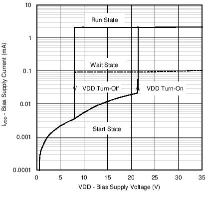 Figure 1. Bias Supply Current vs. Bias Supply Voltage
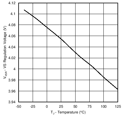 Figure 3. VS Regulation Voltage vs. Temperature
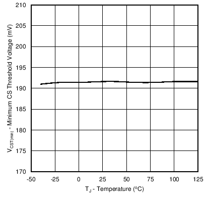 Figure 5. Minimum CS Threshold vs. Temperature
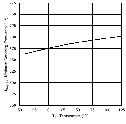
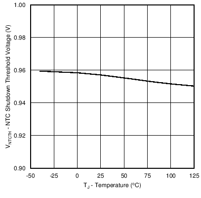 Figure 9. NTC Shutdown Threshold Voltage vs. Temperature
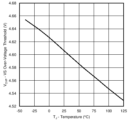 Figure 11. VS Overvoltage Threshold vs. Temperature
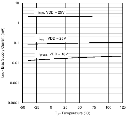 Figure 2. Bias Supply Current vs. Temperature
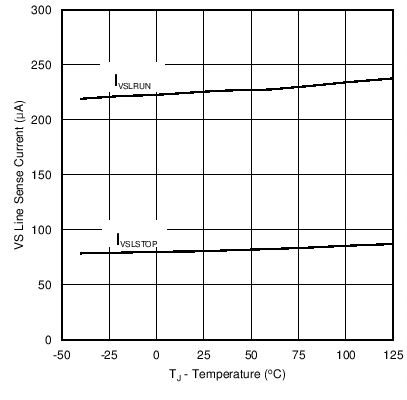 Figure 4. VS Line Sense Current vs. Temperature
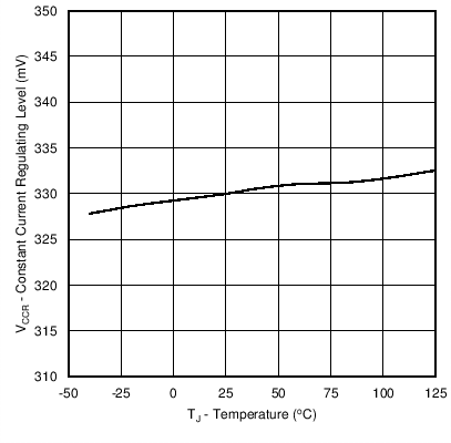 Figure 6. Constant Current Regulating Level vs. Temperature
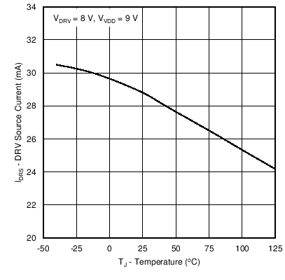
| VDRV = 8 V | VVDD = 9 V |
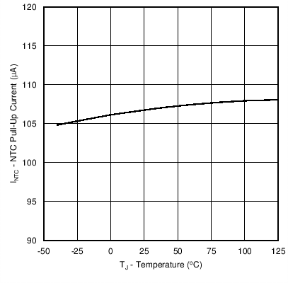 Figure 10. NTC Pull-Up Current vs. Temperature
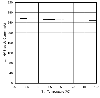 Figure 12. HV Start-Up Current vs. Temperature