ZHCS310G JANUARY 2009 – September 2015 UCC28610
PRODUCTION DATA.
- 1 特性
- 2 应用
- 3 说明
- 4 修订历史记录
- 5 Pin Configuration and Functions
- 6 Specifications
- 7 Detailed Description
- 8 Application and Implementation
- 9 Power Supply Recommendations
- 10Layout
- 11器件和文档支持
- 12机械、封装和可订购信息
7 Detailed Description
7.1 Overview
The flyback converter is attractive for low power AC/DC applications because it provides output isolation and wide input operating abilities using a minimum number of components. Operation of the flyback converter in Discontinuous Conduction Mode (DCM) is especially attractive because it eliminates reverse recovery losses in the output rectifier and it simplifies control.
The UCC28610 is a flyback controller for 12-W to 65-W, peak AC/DC power supply applications that require both low AC line power during no-load operation and high average efficiency. This controller limits the converter to DCM operation. It does not allow Continuous Conduction Mode (CCM) operation. Forced DCM operation results in a uniquely safe current limit characteristic that is insensitive to AC line variations. The peak current mode modulator does not need slope compensation because the converter operates in DCM.
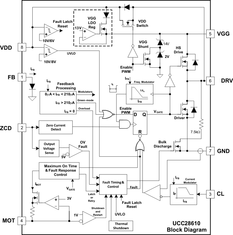
The operation of the UCC28610 is facilitated by driving the external high voltage MOSFET through the source. This configuration is called a cascode driver. It features fast start-up and low input power under no-load conditions without having high voltage connections to the control device. The cascode driver has no effect on the general operation of the flyback converter.
The feedback pin uses current rather than voltage. This unique feature minimizes primary side power consumption during no-load operation by avoiding external resistive conversion from opto-coupler current to voltage.
Average efficiency is optimized by the UCC28610 between peak power and 22% peak power with constant peak current, variable off-time modulation. This modulation tends to make the efficiency constant between 22% and 100% peak load, eliminating the need to over-design to meet average efficiency levels that are required by EnergyStar™.
7.2 Functional Block Diagram
7.3 Feature Description
7.3.1 Fault Recovery
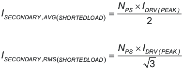
The UCC28610 reacts with the programmed overload response if the overload lasts longer than tOL (nominally 250 ms). The overload fault responses are either (1) latch-off or (2) shutdown/retry after a retry delay of 750 ms. The overload response is programmed with the MOT pin. The forced DCM feature prevents transformer saturation and limits the average and RMS output currents of the secondary winding of the transformer. Even under short circuit load conditions, the output current of the transformer is limited to the levels that are shown in Equation 1, where NPS is the primary-to-secondary turns ratio. Typical behavior for a shorted load is shown in Figure 18.
In shutdown/retry mode switching will be re-enabled after the 750-ms retry delay. In latch-off mode, a 7.5-kΩ load is activated at the DRV pin upon the activation by a fault condition. The internal 7.5-kΩ load draws current from the bulk capacitor through the HVMOSFET and the transformer primary winding. The bias voltage, VDD, is also regulated by the HVMOSFET during the latch-off state. Once the AC line is removed, a 2.8-mA current, IDRV,DSCH, will discharge the bulk capacitor. Ultimately, VDD will discharge when the bulk voltage becomes sufficiently low. A normal start-up cycle can occur if the input voltage is applied after VDD falls below the fault reset level, VDD(FAULT RESET), which is approximately equal to 6 V.
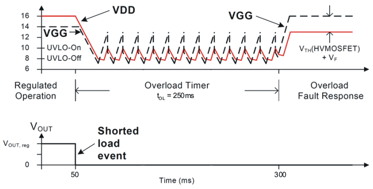 Figure 18. Overload Behavior with a Shorted Output
7.3.2 Maximum On-Time and Brown Out
The forced DCM feature provides protection against excessive primary currents in the event that the input voltage becomes very low. The highest possible secondary currents can be described by Equation 1. The UCC28610 adds further protection by allowing the user to program the maximum on-time.
The Maximum On-Time (MOT) function causes the converter to react as if there is an overload condition if the load is sufficiently large during a line sag condition. During low line conditions the MOT function limits the on-time of the primary switch which limits the peak current in the primary power stage. Figure 19 shows how the MOT period, tMOT, is programmed over the range of 1.5 μs to 5 μs for either range of programming resistors. The resistor range determines the controller’s response to a sustained overload fault – to either Latch-off or to Shutdown/Retry, which is the same response for a line-sag, or brown out, condition.
7.3.3 External Shutdown Using the MOT Pin
Many applications require the ability to shutdown the power supply with external means. This feature is easily implemented by connecting the collector and emitter of an NPN transistor between MOT and GND, respectively. The NPN transistor can be the photo-transistor of an opto-isolator for isolated applications.
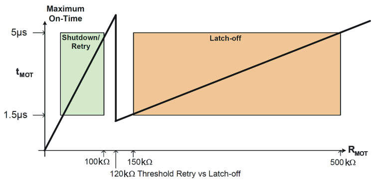 Figure 19. Programming MOT and Overload Fault Response
For latch-off response to over-current or brownout:

where:

For shut-down/retry response to over-current or brownout:

where:

7.3.4 Overvoltage Detection
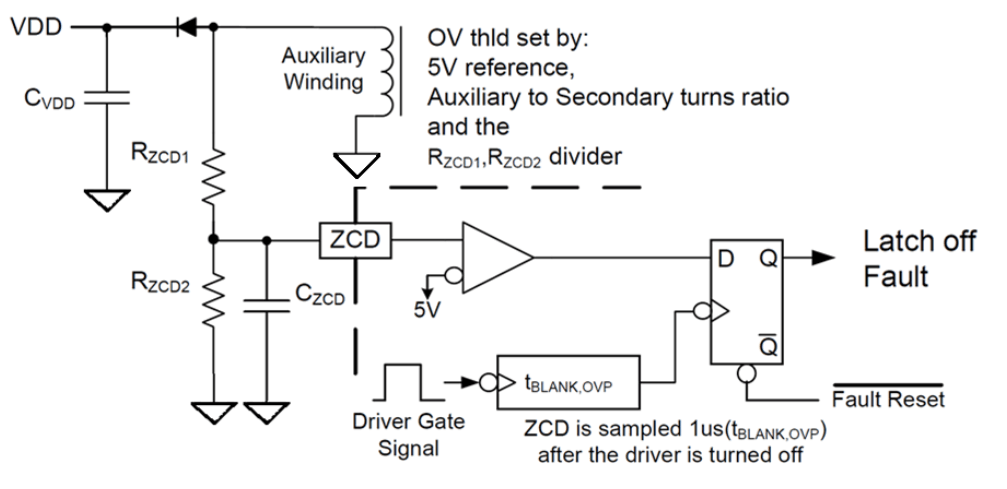
The UCC28610 controller monitors the output voltage by sampling the voltage at the auxiliary winding. The sampling time has a fixed delay of 1 μs, tBLANK,OVP, after the internal driver turns off. This allows the auxiliary winding to be sampled after the bias winding voltage settles from the transient. This same delay is used to blank the ZCD input to avoid unintended zero crossing detection should the ringing be large enough to cross the ZCD zero crossing threshold.
The output over-voltage (OV) threshold is set using the turn ratio of the auxiliary winding to the output secondary and a resistive divider into the ZCD input pin. The UCC28610 will always enter a latched-off state if it detects an OV condition. The VDD supply must cycle below the fault reset threshold to re-start in order to recover. The functionality of the over-voltage detection function is shown in Figure 20.
7.3.5 Solving for High Frequency Ringing
Cascode drive circuits are well known for high speed voltage gain. This topology can have small signal bandwidth well over 100 MHz and it can exhibit high frequency ringing. The internal HS Drive MOSFET shorts the gate to source of the external HVMOSFET during the turn-off interval of the switch cycle. This prevents the HVMOSFET from undesirably exciting the LC resonant circuit in the converter (the magnetizing inductance of the transformer and the stray drain capacitance). High frequency ringing can appear within the built-in dead-time between the turn-off of DRV and the turn-on of the HS Drive. A large amount of energy is transferred through the power components during this dead-time. Excessive high frequency ringing can cause EMI problems and become destructive in some situations.
7.3.5.1 Identification of High Frequency Ringing
The high frequency ringing is the result of stray capacitances ringing with the stray inductance between the source of the HVMOSFET and the DRV pin. Low threshold voltage of the high voltage MOSFET and large peak DRV current can make the ringing worse. In destructive ringing situations, the converter may easily power up and attain regulation the first time, never to start-up again.
The ringing can be observed in either or both of the following conditions:
- The very first HVMOSFET turn-off event during a cold start of the converter (VGG > VDD).
- HVMOSFET turn-off edge under steady state, where the converter switches the HVMOSFET at the programmed IDRV,PK level (VDD > VGG).
7.3.5.2 Avoid HF Ringing
High frequency ringing problems with cascode MOSFET drives can often be avoided. Many converters will not have this problem because they use an HVMOSFET with a large Vth, large RDS(on), low transconductance gain, or operate at low current. Ringing problems can also be avoided by minimizing stray inductance. The trace between the HVMOSFET source and the DRV pin must be kept very short, less than 1 cm. Do not add current probe loops to the source lead of the HVMOSFET. Do not place ferrite beads on the source lead of the HVMOSFET.
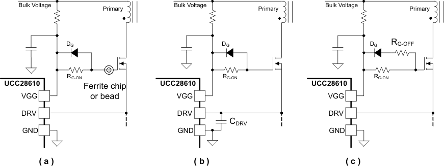
If ringing cannot be avoided, the most efficient and effective methods to solve ringing during switching transients are:
- A ferrite chip or bead connected to the gate of the HVMOSFET,
- A small capacitor connected from DRV to GND and
- A gate turn-off resistor. These three techniques can be used separately or combined, as shown in Figure 21.
7.3.5.3 Ferrite Chip or Bead Solution
The ferrite chip or bead connected to the gate of the HVMOSFET provides the best result because it suppresses ringing in the gate, source, and drain circuits of the HVMOSFET with minimal added losses. Select the ferrite chip for its resistance value in the ringing frequency range (for example, 60 Ω at 100 MHz). The peak current rating of the ferrite chip or bead must be sufficient for the drain – gate discharge current that occurs during the turn-off transient. Excessively large bead reactance can result in low frequency surges of VGG at peak load. Normally, good results can be achieved with a 0603 ferrite chip device.
7.3.5.4 DRV Capacitor Solution
A capacitor between DRV and GND can reduce ringing on VGG. Select the DRV capacitor experimentally by observing the effect on the VGG pin during the first turn-off edge and during the turn-off edge at full load operation. The capacitor should be less than 3.3 nF so that it does not significantly reduce efficiency. Use a capacitor with a low Q, such as one with Y5V dielectric. This technique will not completely damp the ringing yet it can provide sufficient protection against stray inductance between the source of the HVMOSFET and the DRV pin.
7.3.5.5 Gate Turn-Off Resistor Solution
A gate turn-off resistor in the range 0 Ω < RG-OFF < 5 Ω can damp ringing. The turn-off resistance is limited in order to prevent the stray source inductance of the HVMOSFET from over charging VGG through the body diode of the HS Drive MOSFET, in addition to any peak current error problems that would be caused by additional delay. The damping effect of the gate resistor works better in applications with low current and small source inductance.
A much larger resistance can be tolerated during the HVMOSFET turn-on transition due to DCM operation. The recommended turn-on resistance range is 0 Ω <RG-ON < 200 Ω in order to prevent the turn-on delay from interfering with valley switching.
7.3.6 Thermal Shutdown
The UCC28610 protects itself from overheating with an internal thermal shutdown circuit. If the junction temperature exceeds the thermal shutdown point, TSD, the UCC28610 initiates a shutdown event and permits retry after the retry time, tRETRY. Shutdown/Retry cycles continue if the junction temperature is not less than TSD minus TSD_HYST.
7.4 Device Functional Modes
According to the voltage and current among IC pins and the input voltage, output loading conditions, UCC28610 operates in different functional modes.
- At startup, when VDD is below turn on threshold VDD(ON), VGG is clamped at VGG(DISABLED). Flyback MOSFET becomes a source follower with VGG(DISABLED) on its gate. This arrangement allows the VDD capacitor charge up till turn on threshold VGG(ON).
- Once VDD exceed the turn on threshold VGG(ON), the IC start to switching and deliver power to the load. Before IC starts to switching, MOT pin detects its resistor value and set the fault response. Also, the VGG clamp is reduced from VGG(DISABLED) to VGG(OPERATING) to disable the startup operation mode.
- When UCC28610 is switching and deliver power to the load, its switching frequency and peak current are modulated based on FB pin current. The FB pin current is determined by the feedback loop design and output loading condition. During normal operation, the valley switching is
- At heavy load, UCC28610 control the Flyback converter operate at constant peak current with frequency modulation mode (FM) to regulate output voltage.
- In the medium to light load, the converter operate in fixed switching frequency with peak current modeulation mode (AM) to regulate the output voltage.
- Once the load becomes too light, the converter operates in fixed frequency and fixed peak current mode. The output voltage is regulated through burst mode operation.
- UCC28610 can be shut down under different conditions.
- Once the VDD voltage drops below turn off threshold VDD(OFF), UCC28610 shuts down and returns to start up mode.
- If MOT is pulled below 1V externally, UCC28610 shuts down and VDD recycles until MOT pin becomes above 1V to restart.
- If the FB pin current is continuously below IFB(OL) for longer than tOL, UCC28610 shuts down because of over load fault. Depending on the fault response setting, converter either latches off or tries to restart. This fault can be introduced by over load condition or input voltage becomes too low that system loses its capability to regulate output voltage.
- When ZCD pin senses over voltage condition, UCC28610 shuts down. Depending on the fault response setting, UCC28610 enters latch off mode or tries to restart.
- Once internal junction temperature is higher than TSD, UCC28610 shuts down because of over temperature protection. Depending on the fault response setting, UCC28610 latches off or tries to restart after junction temperature drops below TSD-TSD_HYS.
- Once UCC28610 latches off, VDD voltage needs to drop below VDD(FAULT_RESET) to release the latch. During fault reset, input voltage must be disconnected from the source to allow VDD voltage to drop.
