ZHCSBT0D November 2013 – July 2016 UCC28180
PRODUCTION DATA.
- 1 特性
- 2 应用
- 3 说明
- 4 修订历史记录
- 5 说明 (续)
- 6 Pin Configuration and Functions
- 7 Specifications
-
8 Detailed Description
- 8.1 Overview
- 8.2 Functional Block Diagram
- 8.3
Feature Description
- 8.3.1 Soft Start
- 8.3.2 System Protection
- 8.3.3 VCC Undervoltage LockOut (UVLO)
- 8.3.4 Output Overvoltage Protection (OVP)
- 8.3.5 Open Loop Protection/Standby (OLP/Standby)
- 8.3.6 ISENSE Open-Pin Protection (ISOP)
- 8.3.7 ICOMP Open-Pin Protection (ICOMPP)
- 8.3.8 FAULT Protection
- 8.3.9 Output Overvoltage Detection (OVD), Undervoltage Detection (UVD) and Enhanced Dynamic Response (EDR)
- 8.3.10 Overcurrent Protection
- 8.3.11 Soft Overcurrent (SOC)
- 8.3.12 Peak Current Limit (PCL)
- 8.3.13 Current Sense Resistor, RISENSE
- 8.3.14 ISENSE Pin
- 8.3.15 Gate Driver
- 8.3.16 Current Loop
- 8.3.17 ISENSE and ICOMP Functions
- 8.3.18 Pulse Width Modulator
- 8.3.19 Control Logic
- 8.3.20 Voltage Loop
- 8.3.21 Output Sensing
- 8.3.22 Voltage Error Amplifier
- 8.3.23 Non-Linear Gain Generation
- 8.4 Device Functional Modes
-
9 Application and Implementation
- 9.1 Application Information
- 9.2
Typical Application
- 9.2.1 Design Requirements
- 9.2.2
Detailed Design Procedure
- 9.2.2.1 Current Calculations
- 9.2.2.2 Switching Frequency
- 9.2.2.3 Bridge Rectifier
- 9.2.2.4 Inductor Ripple Current
- 9.2.2.5 Input Capacitor
- 9.2.2.6 Boost Inductor
- 9.2.2.7 Boost Diode
- 9.2.2.8 Switching Element
- 9.2.2.9 Sense Resistor
- 9.2.2.10 Output Capacitor
- 9.2.2.11 Output Voltage Set Point
- 9.2.2.12 Loop Compensation
- 9.2.3 Application Curve
- 10Power Supply Recommendations
- 11Layout
- 12器件和文档支持 . .
- 13机械、封装和可订购信息
7 Specifications
7.1 Absolute Maximum Ratings(1)
Over operating free-air temperature range, all voltages are with respect to GND (unless otherwise noted). Currents are positive into and negative out of the specified terminal.| MIN | MAX | UNIT | ||
|---|---|---|---|---|
| Input voltage range | VCC, GATE | –0.3 | 22 | V |
| FREQ, VSENSE, VCOMP, ICOMP | –0.3 | 7 | ||
| ISENSE | –24 | 7 | ||
| Input current range | VSENSE, ISENSE | –1 | 1 | mA |
| Junction temperature, TJ | Operating | –55 | 150 | °C |
| Lead temperature, TSOL | Soldering, 10 s | 300 | °C | |
| Storage temperature, Tstg | –65 | 150 | °C | |
(1) Stresses beyond those listed under “absolute maximum ratings” may cause permanent damage to the device. These are stress ratings only and functional operation of the device at these or any other condition beyond those included under “recommended operating conditions” is not implied. Exposure to absolute-maximum-rated conditions for extended periods of time may affect device reliability.
7.2 ESD Ratings
| VALUE | UNIT | |||
|---|---|---|---|---|
| V(ESD) | Electrostatic discharge | Human-body model (HBM), per ANSI/ESDA/JEDEC JS-001(1) | ±2000 | V |
| Charged-device model (CDM), per JEDEC specification JESD22-C101(2) | ±500 | |||
(1) JEDEC document JEP155 states that 500-V HBM allows safe manufacturing with a standard ESD control process.
(2) JEDEC document JEP157 states that 250-V CDM allows safe manufacturing with a standard ESD control process.
7.3 Recommended Operating Conditions
over operating free-air temperature range (unless otherwise noted)| MIN | MAX | UNIT | ||
|---|---|---|---|---|
| VCC input voltage from a low-impedance source | VCCOFF + 1V | 21 | V | |
| Operating junction temperature, TJ | –40 | 125 | °C | |
| Operating frequency | 18 | 250 | kHz | |
7.4 Thermal Information
| THERMAL METRIC(1) | UCC28180 | UNIT | |
|---|---|---|---|
| D | |||
| 8 PINS | |||
| RθJA | Junction-to-ambient thermal resistance(2) | 116.1 | °C/W |
| RθJCtop | Junction-to-case (top) thermal resistance(3) | 62.2 | |
| RθJB | Junction-to-board thermal resistance(4) | 56.4 | |
| ψJT | Junction-to-top characterization parameter(5) | 14.4 | |
| ψJB | Junction-to-board characterization parameter(6) | 55.9 | |
(1) For more information about traditional and new thermal metrics, see the Semiconductor and IC Package Thermal Metrics application report (SPRA953).
(2) The junction-to-ambient thermal resistance under natural convection is obtained in a simulation on a JEDEC-standard, high-K board, as specified in JESD51-7, in an environment described in JESD51-2a.
(3) The junction-to-case (top) thermal resistance is obtained by simulating a cold plate test on the package top. No specific JEDEC-standard test exists, but a close description can be found in the ANSI SEMI standard G30-88.
(4) The junction-to-board thermal resistance is obtained by simulating in an environment with a ring cold plate fixture to control the PCB temperature, as described in JESD51-8.
(5) The junction-to-top characterization parameter, ψJT, estimates the junction temperature of a device in a real system and is extracted from the simulation data for obtaining RθJA, using a procedure described in JESD51-2a (sections 6 and 7).
(6) The junction-to-board characterization parameter, ψJB, estimates the junction temperature of a device in a real system and is extracted from the simulation data for obtaining RθJA, using a procedure described in JESD51-2a (sections 6 and 7).
7.5 Electrical Characteristics
Unless otherwise noted, VCC=15Vdc, 0.1µF from VCC to GND, –40°C ≤ TJ = TA ≤ +125°C. All voltages are with respect to GND. Currents are positive into and negative out of the specified terminal.| PARAMETER | TEST CONDITIONS | MIN | TYP | MAX | UNIT | |
|---|---|---|---|---|---|---|
| VCC BIAS SUPPLY | ||||||
| ICCPRESTART | ICC Pre-start current | VCC = VCCOFF – 0.2 V | 75 | µA | ||
| ICCSTBY | ICC Standby current | VSENSE = 0.5 V | 1.8 | 2.4 | 3.47 | mA |
| ICCON_load | ICC Operating current | VSENSE = 4.0 V, CGATE = 4.7 nF | 5.8 | 7 | 8.8 | mA |
| UNDER VOLTAGE LOCKOUT (UVLO) | ||||||
| VCCON | VCC Turn on threshold | 10.8 | 11.5 | 12.1 | V | |
| VCCOFF | VCC Turn off threshold | 9.1 | 9.5 | 10.3 | V | |
| UVLO Hysteresis | 1.6 | 1.7 | 2 | V | ||
| VARIABLE FREQUENCY | ||||||
| fSW | Minimum switching frequency | RFREQ = 130 kΩ | 16.3 | 18 | 19.8 | kHz |
| Typical switching frequency | RFREQ = 32.7 kΩ | 61.75 | 65 | 68.25 | kHz | |
| Maximum switching frequency | RFREQ = 8.2 kΩ | 225 | 250 | 275 | kHz | |
| VFREQ | Voltage at FREQ pin | TA = 25°C | 1.43 | 1.5 | 1.56 | V |
| PWM | ||||||
| DMIN | Minimum duty cycle | VSENSE = 5.1 V, ISENSE = –0.25 V | 0% | |||
| DMAX | Maximum duty cycle | VSENSE = 4.0 V, RFREQ = 32.7 Ω | 94.8% | 96.5% | 98% | |
| tOFF(min) | Minimum off time | VSENSE = 3 V, ICOMP = 0.72 V | 450 | 570 | 690 | ns |
| SYSTEM PROTECTION | ||||||
| VSOC | ISENSE threshold, soft over current (SOC) | –0.259 | –0.285 | –0.312 | V | |
| VPCL | ISENSE threshold, peak current limit (PCL) | –0.345 | –0.4 | –0.438 | V | |
| IISOP | ISENSE bias current, ISENSE open-pin protection (ISOP) | ISENSE = 0 V | –2.3 | –2.95 | µA | |
| VISOP | ISENSE threshold, ISENSE open-pin protection (ISOP) | ISENSE = open pin | 0.085 | 0.14 | V | |
| VOLP | VSENSE threshold, open loop protection (OLP) | ICOMP = 1 V, ISENSE = 0 V | 15.6 | 16.5 | 17.6 | %VREF |
| Open loop protection (OLP) Internal pull-down current | VSENSE = 0.5 V | 100 | 325 | nA | ||
| VUVD | VSENSE threshold, output under-voltage detection (UVD) used for enhanced dynamic response(1) | 93.25 | 95 | 97 | %VREF | |
| VOVD | VSENSE threshold, output over-voltage detection (OVD) used for Enhanced dynamic response(1) | 103 | 105 | 106.75 | %VREF | |
| VOVP_L | Output over-voltage protection low threshold, VCOMP is discharged by a 4kΩ resistor when VSENSE > VOVP_L | 105 | 107 | 109 | %VREF | |
| VOVP_H | Output over-voltage protection high threshold, PWM shuts off when VSENSE > VOVP_H | 107 | 109 | 111 | %VREF | |
| VOVP_H(RST) | Output over-voltage protection (VOVP_H) reset threshold, PWM turns on when VSENSE < VOVP_H(RST) | 100 | 102 | 104 | %VREF | |
| ICOMP threshold, external overload protection | 0.2 | 0.25 | %VREF | |||
| CURRENT LOOP | ||||||
| gmi | Transconductance gain | 0.75 | 0.95 | 1.1 | mS | |
| Output linear range (1) | ±50 | µA | ||||
| ICOMP voltage during OLP | VSENSE = 0 V | 2.7 | 3 | 3.3 | V | |
| VOLTAGE LOOP | ||||||
| VREF | Reference voltage | TA = 25°C | 4.93 | 5 | 5.07 | V |
| –40°C ≤ TA ≤ +125°C | 4.87 | 5 | 5.15 | V | ||
| gmv | Transconductance gain without EDR | –40 | –56 | –70 | µS | |
| gmv-EDR | Transconductance gain under EDR | –230 | –280 | –340 | µS | |
| Maximum sink current under normal operation | VSENSE = 5 V, VCOMP = 4 V | 23 | 40 | 57 | µA | |
| Source current under soft start | VSENSE = 4 V, VCOMP = 4 V | –29 | –40 | –52 | µA | |
| Maximum current under EDR operation | VSENSE = 4 V, VCOMP = 2.5 V | –200 | –275 | µA | ||
| VSENSE input bias current | VSENSE = 5 V | 20 | 100 | 250 | nA | |
| VCOMP voltage during OLP | VSENSE = 0.5 V, IVCOMP= 0.5 mA | 0 | 0.04 | 0.10 | V | |
| VCOMP rapid discharge current | VCOMP = 2 V, VCC = floating | 0.37 | mA | |||
| VPRECHARGE | VCOMP precharge voltage | IVCOMP = –100 µA, VSENSE = 4 V | 1.5 | V | ||
| IPRECHARGE | VCOMP precharge current | VCOMP = 0 V | –1 | mA | ||
| VSENSE threshold, end-of-soft-start | Initial Start-up | 98 | %VREF | |||
| GATE DRIVER | ||||||
| GATE current, peak, sinking(1) | CGATE = 4.7 nF | 2 | A | |||
| GATE current, peak, sourcing(1) | CGATE = 4.7 nF | –1.5 | A | |||
| GATE rise time | CGATE = 4.7 nF, GATE = 2 V to 8 V | 8 | 40 | 60 | ns | |
| GATE fall time | CGATE = 4.7 nF, GATE = 8 V to 2 V | 8 | 25 | 40 | ns | |
| GATE low voltage, no load | IGATE = 0 A | 0 | 0.01 | V | ||
| GATE low voltage, sinking | IGATE = 20 mA | 0.04 | 0.06 | V | ||
| GATE low voltage, sourcing | IGATE = -20 mA | –0.04 | –0.06 | V | ||
| GATE low voltage, sinking, OFF | VCC = 5 V, IGATE = 5 mA | 0.1 | 0.2 | 0.31 | V | |
| GATE low voltage, sinking, OFF | VCC = 5 V, IGATE = 20 mA | 0.4 | 0.8 | 1.4 | V | |
| GATE high voltage | VCC = 20 V, CGATE = 4.7 nF | 14.5 | 15.2 | 16.1 | V | |
| GATE high voltage | VCC = 12.2 V, CGATE = 4.7 nF | 10.8 | 11.2 | 12 | V | |
| GATE high voltage | VCC = VCCOFF + 0.2 V, CGATE = 4.7 nF |
8.2 | 9 | 10.1 | V | |
(1) Not production tested. Characterized by design
7.6 Typical Characteristics
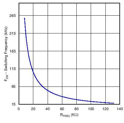
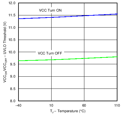
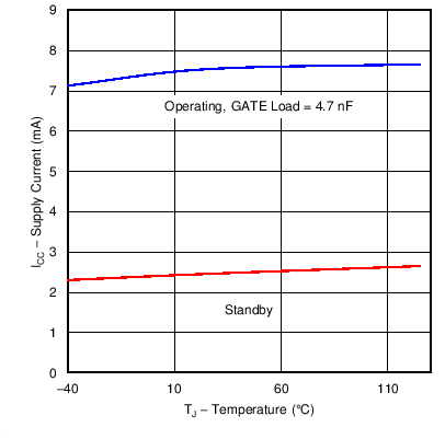
| VCC = 15 V |
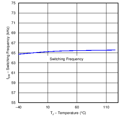
| VCC = 15 V | FSW = 65 kHz |
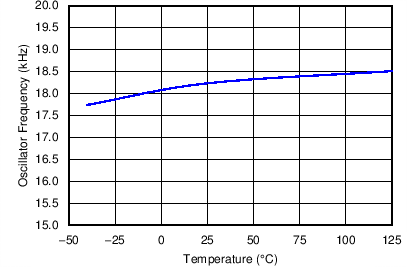
| VCC = 15 V |
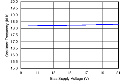
| TJ = 25 °C |
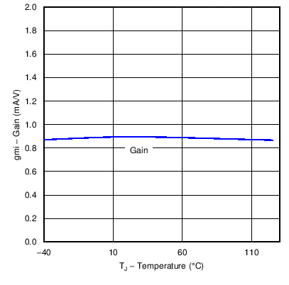
| VCC = 15 V |
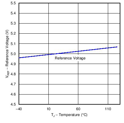
| VCC = 15 V |

| VCC = 15 V |
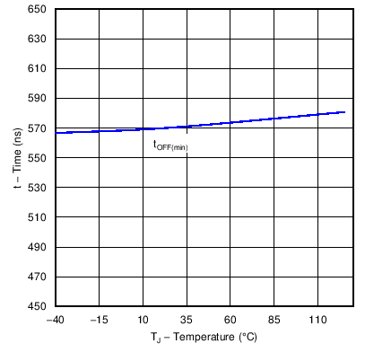
| ICOMP = 0.72 V | VSENSE = 3 V | FSW = 65 kHz |
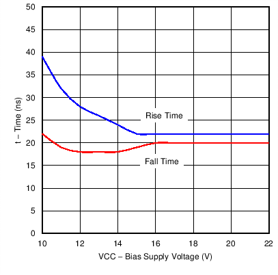
| TJ = 25 °C | CGATE = 4.7 nF | VGATE = 2 V-8 V |
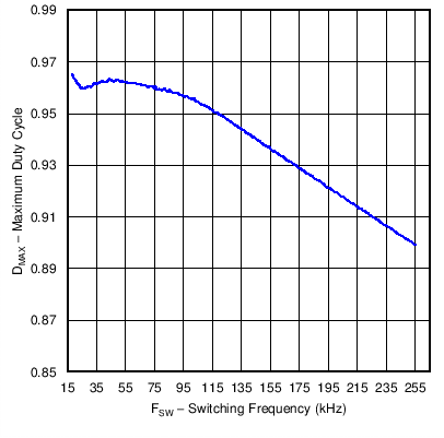
| VCC = 15 V |

| TJ = 25 °C | VSENSE= 3 V | |
| No Gate Load | FSW = 65 kHz |

| VCC = VCCON – 0.2 V | ||
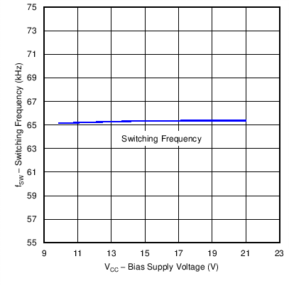
| TJ = 25 °C | FSW = 65 kHz |
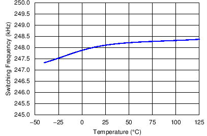
| VCC = 15 V |
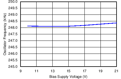
| TJ = 25 °C |
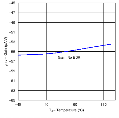
| VCC = 15 V |
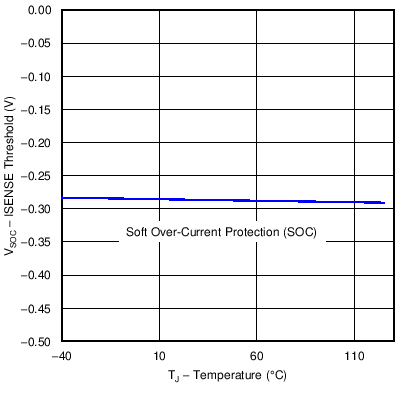
| VCC = 15 V |
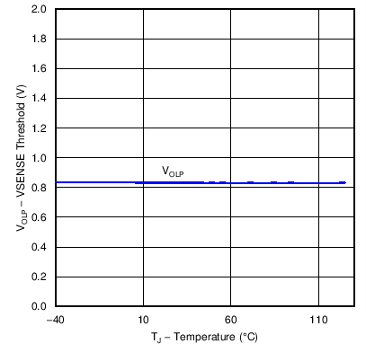
| VCC = 15 V |
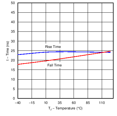
| VCC = 15 V | CGATE = 4.7 nF | VGATE = 2 V-8 V |
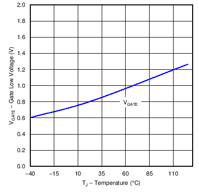
| VCC = 15 V | IGATE = 20 mA |