ZHCSOH9C April 2020 – February 2023 UCC27624
PRODUCTION DATA
- 1 特性
- 2 应用
- 3 说明
- 4 Revision History
- 5 Pin Configuration and Functions
- 6 Specifications
- 7 Detailed Description
- 8 Application and Implementation
- 9 Power Supply Recommendations
- 10Layout
- 11Device and Documentation Support
- 12Mechanical, Packaging, and Orderable Information
封装选项
机械数据 (封装 | 引脚)
散热焊盘机械数据 (封装 | 引脚)
- DGN|8
订购信息
5 Pin Configuration and Functions
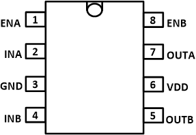
 Figure 5-1 D
Package8-Pin SOICTop View
Figure 5-2 DGN Package8-Pin VSSOPTop View
Table 5-1 Pin Functions
| PIN | TYPE(1) | DESCRIPTION | ||
|---|---|---|---|---|
| NAME | DGN | D | ||
| ENA | 1 | 1 | I | Enable input for Channel A. Biasing ENA, LOW will disable Channel A output regardless of the state of INA. Pulling ENA, HIGH enables the Channel A output. If ENA is left floating, Channel A is enabled by default due to an internal pullup resistor. It is recommended to connect this pin to VDD if unused. |
| ENB | 8 | 8 | I | Enable input for Channel B. Biasing ENB, LOW disables Channel B output regardless of the state of INB. Pulling ENB, HIGH enables the Channel B output. If ENB is left floating, Channel B is enabled by default due to an internal pullup resistor. It is recommended to connect this pin to VDD if unused. |
| GND | 3 | 3 | — | Ground: All signals are referenced to this pin. |
| INA | 2 | 2 | I | Input to Channel A. INA is the non-inverting input of the UCC27624 device. OUTA is held LOW if INA is unbiased or floating by default due to an internal pulldown resistor. Connect this pin to GND if unused. |
| INB | 4 | 4 | I | Input to Channel B. INB is the non-inverting input of the UCC27624 device. OUTB is held LOW if INB is unbiased or floating by default due to an internal pulldown resistor. Connect this pin to GND if unused. |
| OUTA | 7 | 7 | O | Channel A Output |
| OUTB | 5 | 5 | O | Channel B Output |
| VDD | 6 | 6 | I | Bias supply input. Bypass this pin with two ceramic capacitors, generally ≥ 1 μF and 0.1 μF, which are referenced to GND pin of this device. |
| Thermal Pad | — | — | Connect to GND through large copper plane. This pad is not a low-impedance path to GND. | |
(1) I =
Input; O = Output