ZHCSJ21B November   2018  – May 2022 UCC27282

PRODUCTION DATA  

  1. 特性
  2. 应用
  3. 说明
  4. Revision History
  5. Pin Configuration and Functions
  6. Specifications
    1. 6.1 Absolute Maximum Ratings
    2. 6.2 ESD Ratings
    3. 6.3 Recommended Operating Conditions
    4. 6.4 Thermal Information
    5. 6.5 Electrical Characteristics
    6. 6.6 Switching Characteristics
    7. 6.7 Timing Diagrams
    8. 6.8 Typical Characteristics
  7. Detailed Description
    1. 7.1 Overview
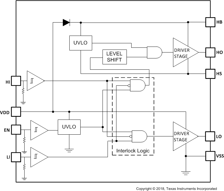
    2. 7.2 Functional Block Diagram
    3. 7.3 Feature Description
      1. 7.3.1 Enable
      2. 7.3.2 Start-up and UVLO
      3. 7.3.3 Input Stages and Interlock
      4. 7.3.4 Level Shifter
      5. 7.3.5 Output Stage
      6. 7.3.6 Negative Voltage Transients
    4. 7.4 Device Functional Modes
  8. Application and Implementation
    1. 8.1 Application Information
    2. 8.2 Typical Application
      1. 8.2.1 Design Requirements
      2. 8.2.2 Detailed Design Procedure
        1. 8.2.2.1 Select Bootstrap and VDD Capacitor
        2. 8.2.2.2 Estimate Driver Power Losses
        3. 8.2.2.3 Selecting External Gate Resistor
        4. 8.2.2.4 Delays and Pulse Width
        5. 8.2.2.5 External Bootstrap Diode
        6. 8.2.2.6 VDD and Input Filter
        7. 8.2.2.7 Transient Protection
      3. 8.2.3 Application Curves
  9. Power Supply Recommendations
  10. 10Layout
    1. 10.1 Layout Guidelines
    2. 10.2 Layout Example
  11. 11Device and Documentation Support
    1. 11.1 Device Support
      1. 11.1.1 第三方产品免责声明
    2. 11.2 接收文档更新通知
    3. 11.3 支持资源
    4. 11.4 Trademarks
    5. 11.5 Electrostatic Discharge Caution
    6. 11.6 术语表
  12. 12Mechanical, Packaging, and Orderable Information

封装选项

机械数据 (封装 | 引脚)
散热焊盘机械数据 (封装 | 引脚)
订购信息

Functional Block Diagram

GUID-306C7A1A-3593-4756-AF59-A1EEB96D8C18-low.gif