ZHCS096B February 2011 – July 2015 UCC27200A , UCC27201A
PRODUCTION DATA.
- 1 特性
- 2 应用
- 3 说明
- 4 修订历史记录
- 5 Pin Configuration and Functions
- 6 Specifications
- 7 Detailed Description
- 8 Application and Implementation
- 9 Power Supply Recommendations
- 10Layout
- 11器件和文档支持
- 12机械、封装和可订购信息
封装选项
机械数据 (封装 | 引脚)
散热焊盘机械数据 (封装 | 引脚)
订购信息
10 Layout
10.1 Layout Guidelines
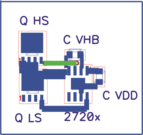
To improve the switching characteristics and efficiency of a design, the following layout rules should be followed.
- Locate the driver as close as possible to the MOSFETs.
- Locate the VDD and VHB (bootstrap) capacitors as close as possible to the driver.
- Pay close attention to the GND trace. Use the thermal pad of the DDA and DRM package as GND by connecting it to the VSS pin (GND). The GND trace from the driver goes directly to the source of the MOSFET but should not be in the high current path of the MOSFET(S) drain or source current.
- Use similar rules for the HS node as for GND for the high side driver.
- Use wide traces for LO and HO closely following the associated GND or HS traces. 60 mil to 100 mil width is preferable where possible.
- Use as least two or more vias if the driver outputs or SW node needs to be routed from one layer to another. For GND the number of vias needs to be a consideration of the thermal pad requirements as well as parasitic inductance.
- Avoid LI and HI (driver input) going close to the HS node or any other high dV/dT traces that can induce significant noise into the relatively high impedance leads.
- Keep in mind that a poor layout can cause a significant drop in efficiency versus a good PCB layout and can even lead to decreased reliability of the whole system.
These references and links to additional information may be found at www.ti.com.
10.2 Layout Example
 Figure 36. Example Component Placement