ZHCSTU3C February 2019 – January 2024 UCC21732-Q1
PRODUCTION DATA
- 1
- 1 特性
- 2 应用
- 3 说明
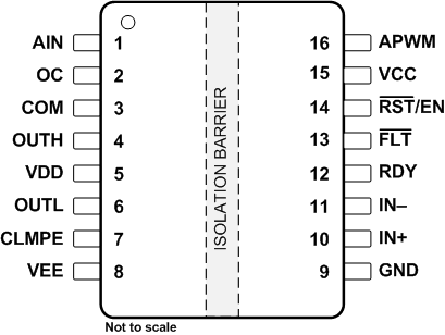
- 4 Pin Configuration and Functions
-
5 Specifications
- 5.1 Absolute Maximum Ratings
- 5.2 ESD Ratings
- 5.3 Recommended Operating Conditions
- 5.4 Thermal Information
- 5.5 Power Ratings
- 5.6 Insulation Specifications
- 5.7 Safety-Related Certifications
- 5.8 Safety Limiting Values
- 5.9 Electrical Characteristics
- 5.10 Switching Characteristics
- 5.11 Insulation Characteristics Curves
- 5.12 Typical Characteristics
- 6 Parameter Measurement Information
-
7 Detailed Description
- 7.1 Overview
- 7.2 Functional Block Diagram
- 7.3
Feature Description
- 7.3.1 Power Supply
- 7.3.2 Driver Stage
- 7.3.3 VCC and VDD Undervoltage Lockout (UVLO)
- 7.3.4 Active Pulldown
- 7.3.5 Short Circuit Clamping
- 7.3.6 External Active Miller Clamp
- 7.3.7 Overcurrent and Short Circuit Protection
- 7.3.8 2-Level Turn-Off
- 7.3.9 Fault ( FLT, Reset and Enable ( RST/EN)
- 7.3.10 Isolated Analog to PWM Signal Function
- 7.4 Device Functional Modes
-
8 Applications and Implementation
- 8.1 Application Information
- 8.2
Typical Application
- 8.2.1 Design Requirements
- 8.2.2
Detailed Design Procedure
- 8.2.2.1 Input Filters for IN+, IN- and RST/EN
- 8.2.2.2 PWM Interlock of IN+ and IN-
- 8.2.2.3 FLT, RDY and RST/EN Pin Circuitry
- 8.2.2.4 RST/EN Pin Control
- 8.2.2.5 Turn-On and Turn-Off Gate Resistors
- 8.2.2.6 External Active Miller Clamp
- 8.2.2.7 Overcurrent and Short Circuit Protection
- 8.2.2.8 Isolated Analog Signal Sensing
- 8.2.2.9 Higher Output Current Using an External Current Buffer
- 9 Power Supply Recommendations
- 10Layout
- 11Device and Documentation Support
- 12Revision History
- 13Mechanical, Packaging, and Orderable Information
3 说明
UCC21732-Q1 是一款电隔离单通道栅极驱动器,旨在用于 SiC MOSFET 和 IGBT,工作电压高达 2121V(直流),具有先进的保护特性、出色的动态性能和稳健性。UCC21732-Q1 具有高达 ±10A 的峰值拉电流和灌电流。
输入侧通过 SiO2 电容隔离技术与输出侧相隔离,支持高达 1.5kVRMS 的工作电压、12.8kVPK 的浪涌抗扰度,隔离栅寿命超过 40 年,并提供较低的器件间偏斜,共模噪声抗扰度 (CMTI) 大于 150V/ns。
UCC21732-Q1 包括先进的保护特性,如快速过流和短路检测、分流电流检测支持、故障报告、有源米勒钳位、输入和输出侧电源 UVLO(用于优化 SiC 和 IGBT 开关行为)和稳健性。可以利用隔离式模拟至 PWM 传感器更轻松地进行温度或电压感测,从而进一步提高驱动器的多功能性并简化系统设计工作量、尺寸和成本。
器件信息
| 器件型号 | 封装(1) | 封装尺寸(标称值) |
|---|---|---|
| UCC21732-Q1 | DW(SOIC,16) | 10.3mm × 7.5mm |
(1) 有关所有可选封装,请参阅 节 13。
器件引脚配置