ZHCSFM4B september 2016 – december 2021 UCC21521
PRODUCTION DATA
- 1 特性
- 2 应用
- 3 说明
- 4 Revision History
- 5 Pin Configuration and Functions
-
6 Specifications
- 6.1 Absolute Maximum Ratings
- 6.2 ESD Ratings
- 6.3 Recommended Operating Conditions
- 6.4 Thermal Information
- 6.5 Power Ratings
- 6.6 Insulation Specifications
- 6.7 Safety-Related Certifications
- 6.8 Safety-Limiting Values
- 6.9 Electrical Characteristics
- 6.10 Switching Characteristics
- 6.11 Insulation Characteristics Curves
- 6.12 Typical Characteristics
- 7 Parameter Measurement Information
- 8 Detailed Description
-
9 Application and Implementation
- 9.1 Application Information
- 9.2
Typical Application
- 9.2.1 Design Requirements
- 9.2.2
Detailed Design Procedure
- 9.2.2.1 Designing INA/INB Input Filter
- 9.2.2.2 Select External Bootstrap Diode and its Series Resistor
- 9.2.2.3 Gate Driver Output Resistor
- 9.2.2.4 Gate to Source Resistor Selection
- 9.2.2.5 Estimate Gate Driver Power Loss
- 9.2.2.6 Estimating Junction Temperature
- 9.2.2.7 Selecting VCCI, VDDA/B Capacitor
- 9.2.2.8 Dead Time Setting Guidelines
- 9.2.2.9 Application Circuits with Output Stage Negative Bias
- 9.2.3 Application Curves
- 10Power Supply Recommendations
- 11Layout
- 12Device and Documentation Support
- 13Mechanical, Packaging, and Orderable Information
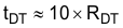
8.4.2.2 DT Pin Connected to a Programming Resistor between DT and GND Pins
To program tDT, place a resistor, RDT, between the DT pin and GND. The appropriate RDT value can be determined from Equation 1, where RDT is in kΩ and tDT in ns:
The steady state voltage at the DT pin is around 0.8 V, and the DT pin current is less than 10 μA when RDT = 100 kΩ. Therefore, it is recommended to parallel a ceramic capacitor, 2.2 nF or above, close to the chip with RDT to achieve better noise immunity and better dead time matching between two channels. Do not leave the DT pin floating.
An input signal’s falling edge activates the programmed dead time for the other signal. The output signals’ dead time is always set to the longer of either the driver’s programmed dead time or the input signal’s own dead time. If both inputs are high simultaneously, both outputs are immediately set low. This feature is used to prevent shoot-through, and it does not affect the programmed dead time setting for normal operation. Various driver dead time logic operating conditions are illustrated in Figure 8-4.
 Figure 8-4 Input and
Output Logic Relationship
with
Input Signals
Figure 8-4 Input and
Output Logic Relationship
with
Input SignalsCondition A: INB goes low, INA goes high. INB sets OUTB low immediately and assigns the programmed dead time to OUTA. OUTA is allowed to go high after the programmed dead time.
Condition B: INB goes high, INA goes low. Now INA sets OUTA low immediately and assigns the programmed dead time to OUTB. OUTB is allowed to go high after the programmed dead time.
Condition C: INB goes low, INA is still low. INB sets OUTB low immediately and assigns the programmed dead time for OUTA. In this case, the input signal’s own dead time is longer than the programmed dead time. Thus, when INA goes high, it immediately sets OUTA high.
Condition D: INA goes low, INB is still low. INA sets OUTA low immediately and assigns the programmed dead time to OUTB. INB’s own dead time is longer than the programmed dead time. Thus, when INB goes high, it immediately sets OUTB high.
Condition E: INA goes high, while INB and OUTB are still high. To avoid overshoot, INA immediately pulls OUTB low and keeps OUTA low. After some time OUTB goes low and assigns the programmed dead time to OUTA. OUTB is already low. After the programmed dead time, OUTA is allowed to go high.
Condition F: INB goes high, while INA and OUTA are still high. To avoid overshoot, INB immediately pulls OUTA low and keeps OUTB low. After some time OUTA goes low and assigns the programmed dead time to OUTB. OUTA is already low. After the programmed dead time, OUTB is allowed to go high.